Your support is needed and is appreciated as Amigaworld.net is primarily dependent upon the support of its users.

|
|
|
|
| Poster | Thread |  cdimauro cdimauro
|  |
Re: The "Let's Buy Commodore" Project
Posted on 17-Jun-2025 4:51:39
| | [ #81 ] |
| |
 |
Elite Member
 |
Joined: 29-Oct-2012
Posts: 4421
From: Germany | | |
|
| @OneTimer1
Quote:
OneTimer1 wrote:
@jingof
Quote:
jingof wrote:
there are only 2 valid candidate answers:
1) to cater to us retro-computing enthusiasts, or
2) to do for the next generation what Commodore did for us (which I posted about here years ago)
(NOTE: You might say I'm missing an option - to build a new, modern computing platform. But I don't think anyone really considers that a realistic goal, and only leads back to people repeating the question "what is the point?".)
...
But who is really focused only delivering a computing platform aimed squarely at children?
|
1. Retro computing enthusiasts are a clear target, according to the videos presented by Peri. he has presented a wide variety of potential products reaching from simple C64 recreations over FPGA based systems up to C64x that are x86 based PCs with Linux.
2. Really next generations that where not listed under 1 could also be a target, but I don't thing the RaspberryPI needs a C= sticker, they where targeted as educational computers and could be used to learn Python (that's what the PI stands for). Python is somehow the BASIC of today with options for building high level applications.
What is missing on Python (in my opinion) are books explaining simple programming but today most of it is done via online tutorials (in text or as video on YT). |
How to Think Like a Computer Scientist
Quote:
But educational platforms doesn't seem to be the target for Peri.'s initiative, they run with or without a C= sticker
|
As usual: to continue milking the cow... |
| | Status: Offline |
| | cdimauro
| |
Re: The "Let's Buy Commodore" Project
Posted on 17-Jun-2025 5:09:17
| | [ #82 ] |
| |
|
Elite Member
|
Joined: 29-Oct-2012
Posts: 4421
From: Germany | | |
|
| @matthey
Quote:
matthey wrote:
cdimauro Quote:
But the problem here is that either you flash the MEGA65 or the C64 core.
You have no chance of using them very quickly, like I did on my C128 (power-on -> native/C128. GO64 or reset + keypress -> C64).
|
It is fast to flash a core, at least compared to 1541 drive times that most C64 users are used to and the timing of which is required for maximum compatibility. The C65 has a GO64 mode too for basic C64 compatibility but full compatibility is not possible without including duplicate C64 hardware. Duplicate hardware including multiple CPUs and video hardware meant the C128 was not cheap. |
You don't need to duplicate the hardware, rather to disable/enable specific features on the fly.
The C128 was >99% compatible with the C64 in C64-mode because of that.
Quote:
| There are rumors that the Amiga 500 ended up cheaper to produce than the C128. |
Hum. Maybe they are just rumours, because I don't find it realistic.
Quote:
| The 68k Amiga SoC that Commodore planned would have dropped the Amiga price by $100 USD according to internal Commodore docs so the Amiga 1200 and CD32 may have ended up cheaper to produce than the C128 too. Even the FPGA based MiSTer+MiSTress A1200 is cheaper than the MEGA65 and can use a C64 or C65 FPGA core which is likely adequate for most Commodore fans. |
Absolutely.
Quote:
cdimauro Quote:
OoOE isn't really important. There are plenty of in-order cores (ARM, RISC-V) which are still sold like pancakes, because they do their job very well and consuming just a fraction of power-hungry OoO cores (which are also fatter -> more expensive).
But yes, other things are important to have.
|
When the instructions and data are cached in L1 (no L1 cache miss stalls) and when there are no load-to-use stalls (68060 design), OoO cores are indeed expensive and wasteful. Most RISC cores have fat code increasing the L1 cache misses and load-to-use stalls which is why they benefit from OoOE removing the excessive stalling. The 68060 has small code with fewer L1 instruction cache misses and avoids load-to-use stalls. |
Yes, but it needs a modern branch predictor with several entries in its cache, a data prefetcher, larger L1 caches (despite the good code density, an increase is required to support more complex code), an L2 cache (at least. L3 might be desirable as well), a return stack, and more entries on the MMU's TLBs.
Quote:
cdimauro Quote:
That's the main concern that I've when Matt shared that the 68060 used a very big 64k x 16-bit LUT for decoding the 68k instructions: I don't know how much impact it could have on the operating frequencies.
|
LUTs are expensive in FPGA because the data is programmable. There is a big difference between what I expect is SRAM for LUTs in a FPGA and read only ROM data in an ASIC. ROM bits in an array can use less than 1 transistor per bit on average. The most common SRAM for CMOS uses 6 transistors/bit (6T SRAM) while 8 transistors/bit (8T SRAM) can reduce power.
https://en.wikichip.org/wiki/static_random-access_memory |
I wasn't referring to SRAM LUTs, but ROM ones, since they are fixed and they are only needed to decode the first 16 bits of a 68k instruction.
The question remains: I don't know if such very big LUT can affect the operating frequencies of the core.
Quote:
| It would be possible to have CPU cores with programmable decoders similar to FPGA programmable logic. This could allow to change ISAs as well as fix bugs which would be convenient but it would likely use more active transistors increasing power. |
Programmable decoders aren't really possible, because each architecture has its own way to map the instructions, and there's no general logic which can accomodate it.
So, a sort of programmability can only come from SRAM's LUTs, which are expensive on both the number of transistors and drawn power.
Quote:
The increased active transistors of CISC decoders are partially offset by the reduced instruction cache and DRAM active transistors. The reduced instruction fetch from a good code density also reduces power and energy used.
https://www.cast-inc.com/blog/consider-code-density-when-choosing-embedded-processors Quote:
Code Densityâs Effect On Power Consumption
A denser instruction set yields smaller code, which in turn requires fewer instruction fetches. This has a major impact on efficiency, because the energy used to fetch an instruction from on-chip memory is much greater than that required for the CPU to execute that instruction.
How much greater? The 2010 Stanford dissertation study by James Balfour on Efficient Embedded Computing showed that for a typical 32-bit RISC processor, an instruction fetch from a 2 Kbyte on-chip cache consumes 6.8 times more energy than a 32-bit add operation (in a typical 45nm CMOS process).
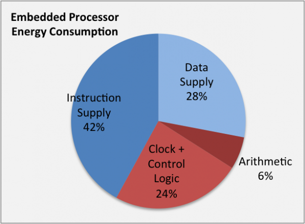
Another study by Dally et al published in IEEE Computer found that 42% of a typical embedded processorâs energy consumption comes from instruction fetching, and only 6% is consumed by performing the actual arithmetic operations.
Both these studies used a small, on-chip cache. When instructions more realistically need to be accessed from larger, on-chip or even worse off-chip memory, the impact is magnified, and the factor of 6.8x can go to 50x or more.
The conclusion here is clear: using an ISA that requires fewer instructions is a much bigger energy saver than simply selecting a processor that executes more efficiently.
|
|
Right, but even taking this into account, a modern CISC processors use a L0 / uop cache to avoid continuously using the decoders, because they draw too much power.
Even some "RISCs" (SIC!) use the same mechanism for the same reasons (since some have quite complicated instructions which are decoded to multiple uops).
Quote:
The 68060 decoders are much different than for x86 yet it does not appear to be an issue in a comparison with the P54C Pentium.
Metric | 68060 | PentiumP54C
Power (max) 5.5W@75MHz 9.5W@75MHz (+73% for Pentium)
Performance (ByteMark-int) 1.20 0.82 (+46% for 68060)
Area (transistors) 2.5million 3.3million (+32% for Pentium)
The 68060 dominated the Pentium in PPA. |
Which is not directly related to the decoders of both.
The Pentium doesn't use so big 64k x 16-bit LUTs for decoding its instructions, but very likely some 256 x 8-bit (or even a bit more than 8-bit, depending from the information that we want to carry out from this analysis), which are quite cheap.
Plus, and this I've already reported it several times, the 68060 cut down several things from the 68k ISA (as per Motorola "tradition", unfortunately") and brought almost nothing new, whereas the Pentium carries ALL x86 legacy and added several other things.
So, a direct comparison of PPA isn't fair. |
| | Status: Offline |
| | Hammer
 | |
Re: The "Let's Buy Commodore" Project
Posted on 17-Jun-2025 12:39:24
| | [ #83 ] |
| |
 |
Elite Member
|
Joined: 9-Mar-2003
Posts: 6484
From: Australia | | |
|
| @cdimauro
Quote:
Then I assume that all those engineers were immediately fired once the C65 was shown to the management, right?
"no new chips" -> they have wasted (a lot of) money of the company going AGAINST such directive.
|
1. CSG LSI group has a different management from the system engineering group's management.
2. CSG LSI group's executive management allowed C65's R&D. In 1989, Herni Rubin allowed AGA R&D due to C65's surprise. Corporate politics is real.
CSG LSI group was responsible for the Vic-20, C64, and C128 that sustained the Commodore group.
The system engineering group was responsible for CBM's 8-bit business desktop computers and C900. C900 advocates are an important factor that will guide the "bet the farm" on ECS and AMIX(UNIX) at the expense of the 256 color 320x200/256 action games use case.
A3000UX + A2408 TiGA is a C900 repeat debacle. Herny Rubin and C900 advocates would rather make AT&T Unix great again instead of focusing on Amiga's core strengths.
Make,
AT&T Unix,
Great,
Again.
vs
Make,
Amiga,
Great,
Again.
3. Commodore's PC business (Jeff Frank) has its system engineering group, e.g. https://theretroweb.com/motherboards/s/commodore-pc-40-iii
Jeff Frank's Commodore PC-40 III used the Western Digital FE3400-10 chipset.
Bill Sydnes and Jeff Frank took over Amiga's system engineering group around June 1991 and froze AGA R&D at the beta state until Mehdi Ali's AA500 directive in February 1992.
Bill Sydnes and Jeff Frank focus on deliving ECS A300/A600, ECS A2200/A2400 (020, Zorro II, cost reduced A3000) and ECS A3200/A3400 (030, Zorro III, cost reduced A3000).
Bill Sydnes and Jeff Frank repeated Henri Rubin's "bet the farm" on ECS and Commodore PC clones overs 256(VGA)/16-bit color(SVGA) use cases.
4. The original Los Gatos Amiga's graphics engineers were kicked out, and its governance was taken over by system engineering (e.g. C= 8-bit business computers and C900).
5. Multimedia group, Irving Gould's protected undermanned group. Rebels from the system engineering group are usually thrown into this group, and they leave Commodore. This group is responsible for CDTV, CDTV-CR with FMV(CL-450 SoC), CD32, FMV module (CL-450 SoC), and CD-1200. Irving Gould would personally fund this group's CD32 production until its very end since He believes MPEG1 VCD is the next best thing. This group selected a custom 40MHz RISC MIPS-X CL-450 SoC. Jeff Porter was thrown into this group around June 1991.
For defending AGA projects and near insubordination, Bill Sydnes kicked Jeff Porter out of the system engineering group and replaced him with Commodore PC's Jeff Frank.
Jeff Frank didn't care about Amiga's chunky pixel issue, hence the A1200 didn't have CD32's hardware C2P. Jeff Frank protects Commodore PC's gaming!
Quote:
IF this directive exists, of course, which I STRONGLY doubt. And that's not only because of the C65 existence, but because of the many chips that Commodore produced AND the general "working model" (!) of Commodore engineers (read Eggebrecht's declaration on the same book AND his interview AND the declaration of Hedley Davis on the same book).
|
You can only conclude that if you didn't read the Commodore - The Final Years book
"Read my lips, no new chips" refers to new graphics hardware context since Herni Rubin allowed 32-bit IO chips R&D to be designed for A3000, but not 32-bit graphics chips e.g. TiGA will handle the business 256 color use case.
https://i.ibb.co/PFWTM8F/AF-072.png
In 1988, Herni Rubin and Commodore Germany would rather demo ATI "business" graphics over Amigas.
Eggebrecht's statement hides behind-the-scenes issues. There are more than 60 projects under Henri Rubin, not focusing on Amiga core graphics R&D.
With C65's surprise, Jeff Porter's 8 bitplane argument for Amiga evolution in 1987 was "I told you so" moment when the system engineering group's management ignored him.
A2000 ECS "productivity mode" was demonstrated to Commodore's executive board in Q4 1988. No-brainer why 1989 released A500 rev6A is a full ECS ready PCB motherboard design, including 512KB ROM support and Agnus B 2MB Chip RAM configuration with jumper settings which didn't exist in A500 Rev 5 board.
1989 released A500 rev6A (and A2000 counterpart) has Agnus B 2MB Chip RAM address line and 512 KB ROM support baked into PCB design.
Another inside story on A3000's full ECS + AmigaOS 2.0 exclusivity debacle and resulting protest and management U-turn.
The inside "read my lips, no new chips" statement requires inside information context, NOT A3000's public product release. There's a reason why CSG's management kept C65 R&D in stealth mode against other Commodore managers.
https://www.appuntidigitali.it/20663/amiga-ecs-and-the-deception-of-read-my-lips-no-new-chips/
your
Quote:
As we can see, then, we are in the presence of new chips that have introduced several new functionalities, whatever Commodoreâs chief engineer might say
|
assertion is without A2000 ECS productivity mode demonstration in Q4 1988 inside information revealed from the Commodore - The Final Years book.
You made your argument in ignorance.
A3000 is just A2000 ECS with A2630 + 32-bit Ramsey + 32-bit FAT Gary + A2320 Amber + non-DMA Zorro III 32-bit Super Buster + SDMAC (for SCSI).
Last edited by Hammer on 18-Jun-2025 at 12:19 AM.
Last edited by Hammer on 17-Jun-2025 at 02:23 PM.
Last edited by Hammer on 17-Jun-2025 at 02:12 PM.
Last edited by Hammer on 17-Jun-2025 at 02:08 PM.
Last edited by Hammer on 17-Jun-2025 at 01:35 PM.
Last edited by Hammer on 17-Jun-2025 at 01:28 PM.
Last edited by Hammer on 17-Jun-2025 at 01:21 PM.
Last edited by Hammer on 17-Jun-2025 at 01:08 PM.
Last edited by Hammer on 17-Jun-2025 at 01:06 PM.
Last edited by Hammer on 17-Jun-2025 at 12:57 PM.
Last edited by Hammer on 17-Jun-2025 at 12:51 PM.
Last edited by Hammer on 17-Jun-2025 at 12:45 PM.
_________________
Amiga 1200 (rev 1D1, KS 3.2, PiStorm32/RPi CM4/Emu68)
Amiga 500 (rev 6A, ECS, KS 3.2, PiStorm/RPi 4B/Emu68)
Ryzen 9 7950X, DDR5-6000 64 GB RAM, GeForce RTX 4080 16 GB |
| | Status: Offline |
| | BigD
| |
Re: The "Let's Buy Commodore" Project
Posted on 17-Jun-2025 22:22:48
| | [ #84 ] |
| |
 |
Elite Member
|
Joined: 11-Aug-2005
Posts: 7551
From: UK | | |
|
| @OneTimer1
Quote:
| The whole "Let's Buy Commodore" project is without the Amiga, Amiga is its own brand and some companies have proven they can sell Amiga compatible retro systems |
Christian mentioned selling a licence to RGL for THECommodore Amiga 1200! He also mentioned merging the Amiga and Commodore IPs again as a long term goal! Amiga is mentioned and on his radar. TBH maybe it is the only way to defeat the Amiga IP squatters to create a large company to withstand and to force them to capitulate and hand back they ill gotten gains but it will take years in the courts!Last edited by BigD on 17-Jun-2025 at 10:24 PM.
_________________
"Art challenges technology. Technology inspires the art."
John Lasseter, Co-Founder of Pixar Animation Studios |
| | Status: Offline |
| | matthey
| |
Re: The "Let's Buy Commodore" Project
Posted on 17-Jun-2025 23:44:00
| | [ #85 ] |
| |
|
Elite Member
|
Joined: 14-Mar-2007
Posts: 2741
From: Kansas | | |
|
| kolla Quote:
A SoC is customized for a particular system with particular features so it can be less desirable for general purpose use. Embedded SoCs especially may discard standard features while adding specialized features. A good example is the embedded SoC used in the A1222 which eliminated the standard PPC FPU along with other desktop features and replaced them with new PPC standards for cheaper embedded hardware. Even the 68040 and 68060 removed support and cut too far for use in embedded markets. It is possible to develop flexible and full featured SoCs which is what I am suggesting.
kolla Quote:
Where would you get this?
|
The 68k CPU cores would be licensed or purchased from NXP if possible. NXP is not making much if anything off the 68k anymore which should reduce the cost of obtaining a license.
kolla Quote:
Where would you get this?
|
Amiga Corporation should own the chipsets and may have more than the schematics. Ideally, Amiga Corporation would be the business developing and producing the 68k SoCs and no license would be required. If a license was required, again the chipsets are making the owner practically nothing right now potentially providing an opportunity to obtain a favorable license.
kolla Quote:
Got details about this?
Which SiFive product or equivalent are you suggesting?
|
Something along the lines of the RISC-V SoC used for the VisionFive 2 sub $100 USD SBC seems appropriate (GPU not included). Maybe some upgraded features would be possible too.
kolla Quote:
Two 68060 cores would be useful for SMP and AMP with the latter more popular for embedded systems. Even the RPi Pico has two Cortex-M cores for the MCUs and not many OSs that would work on the tiny footprint hardware support SMP. I believe SMP would be easier on 68k hardware than PPC hardware. Some hardware features should make SMP support easier as I have suggested before but not everyone likes.
kolla Quote:
Huh, for what? For Legacy? Running separately, with its own RAM? Why just one?
|
The 68000 core would be for maximum compatibility of retro 68000 CPUs but would likely also be used as a very low power I/O and management core. I expect it would access main memory but may be restricted to address ranges and have accesses offset.
kolla Quote:
A 3D core from Imagination Technologies, AMD, Libre-SoC revived, custom, other? Likely not NVidia or ARM.
kolla Quote:
What modern I/O?
What legacy I/O?
|
Modern I/O would be something like what is available on the VisionFive 2. Legacy I/O would be 9-pin game ports, keyboard port, 15-pin VGA, parallel port, IDE port, clock ports and Zorro slots. I like retaining a CD32 compatible PS/2 keyboard/serial port and a clock port. The game ports and 15-pin VGA and parallel ports would likely be on headers but the game ports and 15-pin VGA may be retained or optional for retro use. Maybe the IDE could be converted into a SATA plug to save board space but could still be recognized as IDE on the Amiga. It may not be possible to preserve Zorro and it would likely need quite a bit of logic if it was possible.
kolla Quote:
Hm, modern I/O? I see ISA, ATA, USB 2.0 and 100 Mb ethernet...
|
Look at the newer Vortex86 SoCs. They have both modern and legacy I/O and features for x86(-64). The x86(-64) CPU cores are scalar to reduce power. A modernized superscalar 68060 core would likely be more powerful.
kolla Quote:
Anyways, good luck - better start designing, no time to lose here!
|
The problem is that we have Commodore/Amiga businesses that use branding to sell low value noncompetitive hardware and collusion to keep out competitors. I am suggesting actually producing competitive mass produced Amiga hardware like a legitimate business that may attract younger generations instead of preying on ex-Commodore users. Inconceivable?
|
| | Status: Offline |
| | matthey
| |
Re: The "Let's Buy Commodore" Project
Posted on 18-Jun-2025 2:22:42
| | [ #86 ] |
| |
|
Elite Member
|
Joined: 14-Mar-2007
Posts: 2741
From: Kansas | | |
|
| cdimauro Quote:
You don't need to duplicate the hardware, rather to disable/enable specific features on the fly.
The C128 was >99% compatible with the C64 in C64-mode because of that.
|
No C128 duplication for compatibility?
https://en.wikipedia.org/wiki/Commodore_128#Design Quote:
The C128's complex architecture includes four differently accessed kinds of RAM (128 KB main RAM, 16â64 KB VDC video RAM, 2 kNibbles VIC-II Color RAM, 2-KB floppy-drive RAM on C128Ds, 0, 128 or 512 KB REU RAM), two or three CPUs (main: 8502, Z80 for CP/M; the 128D also incorporates a 6502 in the disk drive), and two different video chips (VIC-IIe and VDC) for its various operational modes.
|
cdimauro Quote:
Hum. Maybe they are just rumours, because I don't find it realistic.
|
I believe it is a plausible claim. The following is the rumored claim with no citation given.
https://en.wikipedia.org/wiki/Commodore_128#Market_performance Quote:
But ultimately the C128 could not compete with the new 16/32-bit systems, which outmatched it and the rest of its 8-bit generation in nearly every aspect. When the C128(D/DCR) was discontinued in 1989, it was reported to cost nearly as much to manufacture as the Amiga 500, even though the C128D had to sell for several hundred dollars less to keep the Amiga's high-end marketing image intact.
|
The C128 may have been cheaper when the Amiga 500 was first released as the C128 chips and parts were older and cheaper but the cost of the Amiga 500 with newer chips and parts would have dropped more and more quickly. The C128 likely reduced Amiga 500 sales that may have increased economies of scale thus reducing costs more quickly so perhaps the C128 should have been discontinued earlier than 1989 or not released at all. Likewise, Commodore 65 development efforts should have gone into the Amiga, especially the AA+ chip development efforts which may have saved Commodore.
cdimauro Quote:
Yes, but it needs a modern branch predictor with several entries in its cache, a data prefetcher, larger L1 caches (despite the good code density, an increase is required to support more complex code), an L2 cache (at least. L3 might be desirable as well), a return stack, and more entries on the MMU's TLBs.
|
The 68060 branch prediction is not bad for an 8-stage pipeline as deeper pipelines need better branch prediction. The combination of static BTFN prediction and dynamic 2-bit saturating prediction provides ~90% prediction accuracy. Still, ColdFireV5 with a 9-stage pipeline improved it.
Introducing the Superscalar Version 5 ColdFire Core Quote:
⢠4-stage, 64-bit Instruction Fetch Pipeline
â Instruction Address Generation
â Instruction Fetch Cycle 1
â Instruction Fetch Cycle 2
â Instruction Early Decode
⢠16-entry FIFO Instruction Buffer: 1 inst/entry
Branch Prediction
â 256-entry, 2-way set-associative branch cache (BCU)
â Local (2-bit state) and 128-entry global predictors
â Folding on predicted-taken branches for 0-cycle execution time
â 2nd-level Branch Acceleration Table used for BCU misses
⢠128-entries, hashed address, 2-bit prediction state
⢠4-entry LIFO Hardware Return Stack
|
This sounds like a two-level adaptive predictor with history which should be good for ~93% prediction accuracy although the BTFN static prediction may improve it more. Instruction fetch was increased to 64-bit/cycle (8B/cycle). A 4-entry LIFO hardware return stack was added although I would like to see that increased to 8-entry which should be trivial. Not mentioned above are the ColdFire 32kiB I+D caches and "32-bit external SDRAM memory" controller. If a license for the ColdFire V5 was obtained too, it could be used to modernize the 68060 quicker. Missing are L2/L3 caches and a stream prefetcher for data. This would then be near the SiFive series 7 technology level.
cdimauro Quote:
I wasn't referring to SRAM LUTs, but ROM ones, since they are fixed and they are only needed to decode the first 16 bits of a 68k instruction.
The question remains: I don't know if such very big LUT can affect the operating frequencies of the core.
|
Also, it would not be 16-bits of the instruction encoding used for the decoding ROM table lookup but more likely 7 or 10 bits. The reg fields would likely not be used.
cdimauro Quote:
Right, but even taking this into account, a modern CISC processors use a L0 / uop cache to avoid continuously using the decoders, because they draw too much power.
Even some "RISCs" (SIC!) use the same mechanism for the same reasons (since some have quite complicated instructions which are decoded to multiple uops).
|
The in-order Bonnell Atom did not break instructions down into microops to save power so it did not use a microop cache.
https://en.wikichip.org/wiki/Bonnell#Front_End Quote:
Front End
Bonnell's front end is very simple when compared to Intel's high-performance architectures. Out-of-order execution (OoOE) that is found ubiquitously in all HPC architectures was rejected. Bonnell's power and area constraints simply couldn't allow for the complex logic needed to support that capability. The Instruction Fetch consists of 3 stages, capable of going through up to 16 bytes per cycle. Like fetch, the Instruction Decode is also 3 stages, capable of decoding instructions with up to 3 prefixes each cycle (considerably longer for more complex instructions).
Bonnell is a departure from all modern x86 architectures with respect to decoding (including those developed by AMD and VIA and every Intel architecture since P6). Whereas modern architectures transform complex x86 instructions into a more easily digestible µop form, Bonnell does almost no such transformations. The pipeline is tailored to execute regular x86 instructions as single atomic operations consisting of a single destination register and up to three source-registers (typical load-operate-store format). Most instructions actually correspond very closely to the original x86 instructions. This design choice results in lower complexity but at the cost of performance reduction. Bonnell has two identical decoders capable of decoding complex x86 instructions. Being variable length instruction architecture introduces an additional layer of complexity. To assist the decoders, Bonnell implements predecoders that determine instruction boundaries and mark them using a single-bit marker. Two cycles are allocated for predecoding as well as L1 storage. Boundary marks are also stored in the L1 eliminating the need to preform needlessly redundant predecoding. Repeated operations are retrieved pre-marked eliminating two cycles. Bonnel has a 36 KiB L1 instruction cache consisting of 32 KiB instruction cache and 4 KiB instruction boundary mark cache. All instructions (coming from both cache or predecode) must undergo full decode. It's worthwhile noting that Intel states Bonnell is a 16-stage pipeline because for the most part, after a cache hit you'll have 16 stages. This is also true in some cases where the processor can simultaneously decode the next instruction. However, in the cases where you get a miss, it will cost 3 additional stages to catch up and locate the boundary for that instruction for a total of 19 stages.
Some x86 instructions are simply too complex to handle directly. Those selected few get diverted into the micro-code sequencer ROM (MSROM) for decoding producing much more sane RISCish instructions at the cost of 2 additional cycles. Intel estimates that only 5% of common software require instructions to be split up. Only decoder0 can request transfer to use the MSROM. All instructions longer than 8 bytes or instructions having more than three prefixes will result in a MSROM transfer unconditionally. Those instructions will experience two cycles of delay. The inability to execute things out-of-order eliminates lots of optimization opportunities at this stage. One thing Bonnell can do is lockstep instructions that can be execute simultaneously such as in the case of instructions that performance a memory access along an arithmetic operation. In those instances Bonnell will issue the instruction as if it were two separate instructions executing simultaneously. In addition, only one x87 instruction can be decoded per cycle.
Because Bonnell has support for Hyper-Threading, Intel's brand name for their own simultaneous multithreading technology, a number of modifications had to be done. The prefetch buffer and the instruction queue have been duplicated for each thread.
|
Breaking instructions down into microops improves performance, especially for a non-orthogonal ISA, but it requires more power for decoding which the microop cache partially offsets. Bonnell adds a boundary mark cache to reduce the decoding overhead of finding the instruction length. The 68060 could easily add a boundary mark cache too but I doubt it would be necessary because the length of most 68k instructions is known by examining the first 16-bits (90+% of instructions?). The 68k instructions that are not use less common addressing modes with brief or full extension word formats. The 68060 likely decodes up to 30% fewer instructions than x86 only Bonnell with only 8 GP registers which also increases power for memory traffic. Despite Bonnell x86 handicaps, a Bonnell core is similar to what is wanted for an upgraded 68060 core other than SMT but is only 500 mW to 2 W TDP per core using a 45nm process.
Quote:
Architecture
Strictly ultra-low power
o 90%+ lower power than 90 nm Pentium M
45 nm process, 9 metal layers, CMOS
500 mW to 2 W TDP
o Average 220 mW
o Idle under 80 mW
533 MT/s dual mode (GTL & CMOS) FSB
In-order
2-issue decode
Simple 2-way SMT
Instruction Queue of 32 entries (16 entries/thread)
FP Register File (per thread)
Integer Register File (per thread)
Private L1 cache for each core
Shared L2 cache for the entire chip
The number of functional units were kept to minimum to cut on power consumption.
2 address generation units (AGUs)
2 Integer ALUs (1 for jumps, 1 for shifts)
2 FP ALUs (1 adder, 1 for others)
No Integer multiplier & divider (shared with FP ALU instead)
|
Despite low power compromises, in-order Bonnell Atom cores had enough performance and power efficiency to compete with ARM OoO cores. Remember these benchmarks (lower is better).

https://www.extremetech.com/extreme/188396-the-final-isa-showdown-is-arm-x86-or-mips-intrinsically-more-power-efficient
The closest competition for the 2-way in-order Bonnell Atom from ARM is the 3-way OoO Cortex-A15. The in-order 2-way Cortex-A53 is about the same performance as the crushed 2-way OoO Cortex-A9 while using less power and area.
https://chipsandcheese.com/p/arms-cortex-a53-tiny-but-important Quote:
But design paradigms that fail in one sector typically donât fall off the face of the earth. Instead, they find a niche elsewhere, and continue to play a role in our lives even if itâs not flashy enough to dominate headlines. ARMâs Cortex A53 is an excellent example. Avoiding the power and area of out-of-order execution still matters when youâre targeting power levels at 1 watt and below, and trying to save every last bit of core area. The in-order versus out-of-order debate didnât end. Instead, it was pushed down to lower power and performance points. According to ARMâs keynote presentation, Cortex A53 can deliver the same performance as the 2-wide, out-of-order Cortex A9 while being 40% smaller on the same 32 nm process.
|
CISC in-order cores can replace RISC OoO cores although it helps to start with a more efficient CISC ISA than x86(-64). Even fat in-order x86 cores can do it below where they scale easily.
cdimauro Quote:
Which is not directly related to the decoders of both.
The Pentium doesn't use so big 64k x 16-bit LUTs for decoding its instructions, but very likely some 256 x 8-bit (or even a bit more than 8-bit, depending from the information that we want to carry out from this analysis), which are quite cheap.
Plus, and this I've already reported it several times, the 68060 cut down several things from the 68k ISA (as per Motorola "tradition", unfortunately") and brought almost nothing new, whereas the Pentium carries ALL x86 legacy and added several other things.
So, a direct comparison of PPA isn't fair.
|
Bonnell Atom cores with more modern x86 support than the original Pentium are fatter than any 68k support that would be added back into 68060 cores (Bonnell ~14 million transistors vs 68060 ~2.5 million transistors). The fat Bonnell cores are likely the reason why SMT was used where the ARM core competition does not use SMT and the more expensive price with bloated Bonnell cores reduced the price efficiency even though the performance and power efficiency were often better than ARM cores. Intel tried to stay with x86 for Bonnell because of the big jump in bloat and complexity with x86-64 but too much of the x86 software had been upgraded to x86-64 and that is what customers wanted, resulting in the lowest power x86 Bonnell cores going away.
Last edited by matthey on 18-Jun-2025 at 01:47 PM.
Last edited by matthey on 18-Jun-2025 at 02:47 AM.
Last edited by matthey on 18-Jun-2025 at 02:40 AM.
|
| | Status: Offline |
| | matthey
| |
Re: The "Let's Buy Commodore" Project
Posted on 18-Jun-2025 5:00:10
| | [ #87 ] |
| |
|
Elite Member
|
Joined: 14-Mar-2007
Posts: 2741
From: Kansas | | |
|
| BigD Quote:
Christian mentioned selling a licence to RGL for THECommodore Amiga 1200! He also mentioned merging the Amiga and Commodore IPs again as a long term goal! Amiga is mentioned and on his radar. TBH maybe it is the only way to defeat the Amiga IP squatters to create a large company to withstand and to force them to capitulate and hand back they ill gotten gains but it will take years in the courts! |
Larger is not necessarily stronger. If My Retro Computer Ltd was financially strong, then they would not need to raise money through crowd funding. If they sold competitive hardware, then they would not be as reliant on the Commodore brand. If they were not desperate, they likely would not offer Christian a CEO job if he raised enough money for them.
The Commodore brand would not help Michele fight off the Amiga IP squatters. I believe he would prevail in court anyway but it is more likely Hyperion will go bankrupt or negotiate a settlement first. A settlement may be the best outcome for Hyperion and their negotiating position becomes weaker the closer we get to the next trial. If they think they can wait until the last moment to negotiate, Michele may just wait to see the verdict. Too bad Michele can not get blood from the turnip that Hyperion is but there may be enough criminality to pierce the corporate veil and go after Hyperion stockholders, officers and directors.
https://blacks_law.en-academic.com/37530/piercing_the_corporate_veil Quote:
piercing the corporate veil
Judicial process whereby court will disregard usual immunity of corporate officers or entities from liability for wrongful corporate activities; e.g. when incorporation exists for sole purpose of perpetrating fraud. The doctrine which holds that the corporate structure with its attendant limited liability of stockholders may be disregarded and personal liability imposed on stockholders, officers and directors in the case of fraud or other wrongful acts done in name of corporation. The court, however, may look beyond the corporate form only for the defeat of fraud or wrong or the remedying of injustice. Hanson v. Bradley, 298 Mass. 371, 381, 10 N.E.2d 259, 264.
|
Hyperion used to have a legit game porting business until Ben realized it was not profitable and the way to survive in the Amiga market was to steal from other businesses.
|
| | Status: Offline |
| | Hammer
| |
Re: The "Let's Buy Commodore" Project
Posted on 18-Jun-2025 7:53:28
| | [ #88 ] |
| |
|
Elite Member
|
Joined: 9-Mar-2003
Posts: 6484
From: Australia | | |
|
| @matthey
Quote:
A SoC is customized for a particular system with particular features so it can be less desirable for general purpose use. Embedded SoCs especially may discard standard features while adding specialized features. A good example is the embedded SoC used in the A1222 which eliminated the standard PPC FPU along with other desktop features and replaced them with new PPC standards for cheaper embedded hardware. Even the 68040 and 68060 removed support and cut too far for use in embedded markets. It is possible to develop flexible and full featured SoCs which is what I am suggesting.
|
PPC e500's custom FPU was ditched by the supplier. The work for A1222's custom FPU emulating a normal FPU was effectively wasted.
Quote:
The 68k CPU cores would be licensed or purchased from NXP if possible. NXP is not making much if anything off the 68k anymore which should reduce the cost of obtaining a license.
|
Rochester Electronics has a 68040 license, and it's not price vs performance competitive. The ex-Motorola employee, Curt Gerrish founded Rochester Electronics has passed away in Dec 2024, age of 88.
Curt's sons, Chris and Paul Gerrish lead Rochester Electronics.
_________________
Amiga 1200 (rev 1D1, KS 3.2, PiStorm32/RPi CM4/Emu68)
Amiga 500 (rev 6A, ECS, KS 3.2, PiStorm/RPi 4B/Emu68)
Ryzen 9 7950X, DDR5-6000 64 GB RAM, GeForce RTX 4080 16 GB |
| | Status: Offline |
| | number6
| |
Re: The "Let's Buy Commodore" Project
Posted on 21-Jun-2025 12:34:45
| | [ #89 ] |
| |
 |
Elite Member
|
Joined: 25-Mar-2005
Posts: 11856
From: In the village | | |
|
| @thread
Commodore patreon posts about his history and Peri's Commodore project:
AtariAge thread on topic
#6 _________________
This posting, in its entirety, represents solely the perspective of the author.
*Secrecy has served us so well* |
| | Status: Offline |
| | number6
| |
Re: The "Let's Buy Commodore" Project
Posted on 21-Jun-2025 14:48:36
| | [ #90 ] |
| |
|
Elite Member
|
Joined: 25-Mar-2005
Posts: 11856
From: In the village | | |
|
| @thread
embedded link in AtariAge (above) Link to new article on topic courtesy Commodore patreon Chijanofuji
A discussion with Christian âPeri Fracticâ Simpson
#6
Added: Pass protected site now up:
Here Last edited by number6 on 21-Jun-2025 at 02:52 PM.
_________________
This posting, in its entirety, represents solely the perspective of the author.
*Secrecy has served us so well* |
| | Status: Offline |
| | matthey
| |
Re: The "Let's Buy Commodore" Project
Posted on 21-Jun-2025 22:54:51
| | [ #91 ] |
| |
|
Elite Member
|
Joined: 14-Mar-2007
Posts: 2741
From: Kansas | | |
|
| #6 Quote:
Chijanofuji claims to be supporting Peri's Patreon.
https://forums.atariage.com/topic/382268-can-we-save-commodore/page/3/#elControls_5678746_menu
Chijanofuji Quote:
mr_me Quote:
Does it matter that your TheC64 doesn't say Commodore on it?
|
Yes it does to me. The actual Commodore name and logo would have made it even better. Not to the point where I would have gone out to buy an otherwise completely not relevant to Commodore product like the Commodore PET smartphone that was out in 2015/2016 just to have the name and logo on it, but still...
|
Criticizing the Commodore PET smartphone as a product "completely not relevant to Commodore" but supporting Peri's efforts with his connection to My Retro Computer Ltd and the Commodore C64x product which is "completely not relevant to Commodore" seems hypocritical to me.
#6 Quote:
Peri Fractic Quote:
5 Will there be new hardware? Nothing has officially been announced, but given that this all started because My Retro Computer licensed the Commodore name for a hardware product, it certainly seems possible. And the prospect of future tech isnât off the table, either. Peri Fractic points to the company Voxon, which builds a 3D hologram display, as an inspiration of sorts. âThatâs the kind of stuff that feels like it would be what Commodore would make,â he says.
|
Invest in hardware that "feels like it would be what Commodore would make" including a 3D hologram display and My Retro Computer Ltd x86-64 hardware with Linux. The Commodore PET smartphone is a product "completely not relevant to Commodore" though.
#6 Quote:
Added: Pass protected site now up:
Here
|
The website tab is misspelled "Commdore" and the password protected homepage sends a message about openness. Sigh.
|
| | Status: Offline |
| | number6
| |
Re: The "Let's Buy Commodore" Project
Posted on 21-Jun-2025 23:14:51
| | [ #92 ] |
| |
|
Elite Member
|
Joined: 25-Mar-2005
Posts: 11856
From: In the village | | |
|
| @matthey
I understand your post in its entirety. The notion that Peri would be communicating with Commodore Inc./Industries/Engineering and yet be somehow less interested in communicating with the CBM branch (formerly CommodoreSmart).
I realize your question relates to Sean and the C64, but it's the same question when it comes to CBM branch.
Perhaps all my posts about CBM's on again off again filings? Nostalgia Nerd also raised some questions about those actions. dunno. Let's not conclude anything just yet.
Regardless, this is what caught my eye:
Quote:
| Peri Fractic says he has been in touch with Mike Battilana, the owner of the Amiga brand and its primary software distributor, Cloanto. âMike and I are probably the two people who share that strongest will to put the pieces of the jigsaw back together,â he says. |
You might recall initially Peri did some "name dropping". But the above seems a bit bolder statement concerning Mike.
This is still evolving. I see some corrections and/or changes starting to appear as well.
#6
Added: The original text concerning the date of the next video was July 28. This has now been changed to June 28.
Quote:
| Correction: An earlier version of this piece stated the wrong publish date for Peri Fracticâs next video. Itâs expected to show up on June 28. We regret the error. |
Last edited by number6 on 21-Jun-2025 at 11:37 PM.
Last edited by number6 on 21-Jun-2025 at 11:19 PM.
_________________
This posting, in its entirety, represents solely the perspective of the author.
*Secrecy has served us so well* |
| | Status: Offline |
| | matthey
| |
Re: The "Let's Buy Commodore" Project
Posted on 22-Jun-2025 5:59:43
| | [ #93 ] |
| |
|
Elite Member
|
Joined: 14-Mar-2007
Posts: 2741
From: Kansas | | |
|
| #6 Quote:
I understand your post in its entirety. The notion that Peri would be communicating with Commodore Inc./Industries/Engineering and yet be somehow less interested in communicating with the CBM branch (formerly CommodoreSmart).
I realize your question relates to Sean and the C64, but it's the same question when it comes to CBM branch.
Perhaps all my posts about CBM's on again off again filings? Nostalgia Nerd also raised some questions about those actions. dunno. Let's not conclude anything just yet.
|
I am not saying the CBM branch of people should necessarily be involved in the unification of Commodore, although if they are still active it would be good to communicate with them and try to earn their acceptance at least. My point was that their Commodore PET smartphone may have been as legitimate as any other Commodore themed hardware with Commodore branding including the My Retro Computer Ltd Commodore 64x. Peri makes it sound like we would have the official line of Commodore branding, trademarks and copyrights with heritage from Commodore, at least with Mike Battilana's involvement, but is that more important than faithful hardware or will hardware with a competing heritage suffice to replace it? Did x86 win because it was superior to the 68k or because Motorola tossed their beautiful baby out with the bathwater do to AIM Alliance politics? Did the x86(-64) BIOS/UEFI win because it was better than the Amiga chipset or was Commodore just too slow and incompetent to upgrade it? Will it be accepted by Commodore fans to throw out the better hardware heritage and accept the inferior competing hardware for the Commodore/Amiga replacement?
#6 Quote:
Regardless, this is what caught my eye:
Quote:
| Peri Fractic says he has been in touch with Mike Battilana, the owner of the Amiga brand and its primary software distributor, Cloanto. âMike and I are probably the two people who share that strongest will to put the pieces of the jigsaw back together,â he says. |
You might recall initially Peri did some "name dropping". But the above seems a bit bolder statement concerning Mike.
This is still evolving. I see some corrections and/or changes starting to appear as well.
|
For other people trying to follow this discussion, your quote from above is one of the five questions about the Commodore acquisition from a recent link you posted.
https://tedium.co/2025/06/19/peri-fractic-retro-recipes-commodore-profile/ Quote:
1 What about the Amiga? The Commodore brand was separated from the Amiga line nearly three decades ago, and while the Amiga has slowed somewhat in recent years, the scene is very much alive. Peri Fractic says he has been in touch with Mike Battilana, the owner of the Amiga brand and its primary software distributor, Cloanto. âMike and I are probably the two people who share that strongest will to put the pieces of the jigsaw back together,â he says.
|
Peri has dropped several big names in the retro Commodore/Amiga Community including Mike Battilana, Jeri Ellsworth and Bil Herd while it is unclear how much communication he has had with them and how much support he has gained from them. I believe all these people are good people with good intentions but that does not mean they are fully committed to helping Peri achieve his goal of a reunited Commodore. Maybe Peri had an epiphany moment to restore Commodore but motivation without direction will likely fail. I have doubts about his priority goal of buying the Commodore brand, his alliance with My Retro Computer Ltd and Peri himself. I do not doubt his ambition though and maybe something good will come from this.
|
| | Status: Offline |
| | number6
| |
Re: The "Let's Buy Commodore" Project
Posted on 22-Jun-2025 15:05:19
| | [ #94 ] |
| |
|
Elite Member
|
Joined: 25-Mar-2005
Posts: 11856
From: In the village | | |
|
| @matthey
You can take it a step further. These people all know each other. It's not like this effort sprang out of thin air. David Pleasance has spoken with one branch of Commodore by his own admission. Trevor Dickinson has spoken with Sean Donohue, etc.
Name dropping vs substantive results. Sure. We don't have a handle on that atm, but in less than a week we should have more detail to banter around.
#6 _________________
This posting, in its entirety, represents solely the perspective of the author.
*Secrecy has served us so well* |
| | Status: Offline |
| | cdimauro
| |
Re: The "Let's Buy Commodore" Project
Posted on 23-Jun-2025 20:18:21
| | [ #95 ] |
| |
|
Elite Member
|
Joined: 29-Oct-2012
Posts: 4421
From: Germany | | |
|
| @Hammer
Quote:
Hammer wrote:
@cdimauro
Quote:
Then I assume that all those engineers were immediately fired once the C65 was shown to the management, right?
"no new chips" -> they have wasted (a lot of) money of the company going AGAINST such directive.
|
1. CSG LSI group has a different management from the system engineering group's management.
2. CSG LSI group's executive management allowed C65's R&D. |
Source for this? In the past I've already asked you who ordered starting the C65, but you haven't provided any detail.
Now you talk of a generic "executive management", which remains cloudy (at least).
Quote:
In 1989, Herni Rubin allowed AGA R&D due to C65's surprise. Corporate politics is real.
CSG LSI group was responsible for the Vic-20, C64, and C128 that sustained the Commodore group.
The system engineering group was responsible for CBM's 8-bit business desktop computers and C900. C900 advocates are an important factor that will guide the "bet the farm" on ECS and AMIX(UNIX) at the expense of the 256 color 320x200/256 action games use case.
A3000UX + A2408 TiGA is a C900 repeat debacle. Herny Rubin and C900 advocates would rather make AT&T Unix great again instead of focusing on Amiga's core strengths.
Make,
AT&T Unix,
Great,
Again.
vs
Make,
Amiga,
Great,
Again.
3. Commodore's PC business (Jeff Frank) has its system engineering group, e.g. https://theretroweb.com/motherboards/s/commodore-pc-40-iii
Jeff Frank's Commodore PC-40 III used the Western Digital FE3400-10 chipset.
Bill Sydnes and Jeff Frank took over Amiga's system engineering group around June 1991 and froze AGA R&D at the beta state until Mehdi Ali's AA500 directive in February 1992.
Bill Sydnes and Jeff Frank focus on deliving ECS A300/A600, ECS A2200/A2400 (020, Zorro II, cost reduced A3000) and ECS A3200/A3400 (030, Zorro III, cost reduced A3000).
Bill Sydnes and Jeff Frank repeated Henri Rubin's "bet the farm" on ECS and Commodore PC clones overs 256(VGA)/16-bit color(SVGA) use cases.
4. The original Los Gatos Amiga's graphics engineers were kicked out, and its governance was taken over by system engineering (e.g. C= 8-bit business computers and C900).
5. Multimedia group, Irving Gould's protected undermanned group. Rebels from the system engineering group are usually thrown into this group, and they leave Commodore. This group is responsible for CDTV, CDTV-CR with FMV(CL-450 SoC), CD32, FMV module (CL-450 SoC), and CD-1200. Irving Gould would personally fund this group's CD32 production until its very end since He believes MPEG1 VCD is the next best thing. This group selected a custom 40MHz RISC MIPS-X CL-450 SoC. Jeff Porter was thrown into this group around June 1991.
For defending AGA projects and near insubordination, Bill Sydnes kicked Jeff Porter out of the system engineering group and replaced him with Commodore PC's Jeff Frank. |
According to the above, Sydnes arrived only on June 1991.
It would be interesting to know what the Amiga engineers have done before that, since on September 1987 they've already started discussing about the "next big thing", and after FOUR years they've produced... what?
Quote:
| Jeff Frank didn't care about Amiga's chunky pixel issue, hence the A1200 didn't have CD32's hardware C2P. Jeff Frank protects Commodore PC's gaming! |
According to YOUR "hero", the Amiga engineers already knew 1-2 years before the CD32 how chunky pixels were important for the 3D, but what they have done was... NOTHING!
That logic on Akiko was talked during a lunch break and implemented in one day. With which managers it was discussed BEFORE working on it? WHO from the management has approved it?
Quote:
Quote:
IF this directive exists, of course, which I STRONGLY doubt. And that's not only because of the C65 existence, but because of the many chips that Commodore produced AND the general "working model" (!) of Commodore engineers (read Eggebrecht's declaration on the same book AND his interview AND the declaration of Hedley Davis on the same book).
|
You can only conclude that if you didn't read the Commodore - The Final Years book |
I've read enough from that, which is NOT the bible on this argument, BTW.
In fact, the NEW chips developed by Commodore are a clear statement against this imaginative directive, which likely was invented by some engineer to justify their incompetence.
Quote:
"Read my lips, no new chips" refers to new graphics hardware context since Herni Rubin allowed 32-bit IO chips R&D to be designed for A3000, but not 32-bit graphics chips e.g. TiGA will handle the business 256 color use case.
https://i.ibb.co/PFWTM8F/AF-072.png |
I already know this picture, which I've used on my article. For the rest... see above.
Quote:
In 1988, Herni Rubin and Commodore Germany would rather demo ATI "business" graphics over Amigas.
Eggebrecht's statement hides behind-the-scenes issues. There are more than 60 projects under Henri Rubin, not focusing on Amiga core graphics R&D. |
Nevertheless, he was talking about the engineers he worked with.
Besides that, you're still carefully avoiding what Hedley Davis said about the general "policy" at Commodore. Guess why: because it's not supporting your propaganda.
Quote:
| With C65's surprise, Jeff Porter's 8 bitplane argument for Amiga evolution in 1987 was "I told you so" moment when the system engineering group's management ignored him. |
On 1987 even the stones knew that 256 colours were absolutely needed...
Quote:
A2000 ECS "productivity mode" was demonstrated to Commodore's executive board in Q4 1988. No-brainer why 1989 released A500 rev6A is a full ECS ready PCB motherboard design, including 512KB ROM support and Agnus B 2MB Chip RAM configuration with jumper settings which didn't exist in A500 Rev 5 board.
1989 released A500 rev6A (and A2000 counterpart) has Agnus B 2MB Chip RAM address line and 512 KB ROM support baked into PCB design. |
And what's the point here? If the chips are pin-compatible then you can design the PCB for supporting future chips even with completely new features.
Quote:
| Another inside story on A3000's full ECS + AmigaOS 2.0 exclusivity debacle and resulting protest and management U-turn. |
Well, ECS was 16-bit chipset: "great innovation" from the OCS one, and a "great chipset" for a 32-bit system...
Quote:
| The inside "read my lips, no new chips" statement requires inside information context, NOT A3000's public product release. There's a reason why CSG's management kept C65 R&D in stealth mode against other Commodore managers. |
Same as above: source for this?
Quote:
https://www.appuntidigitali.it/20663/amiga-ecs-and-the-deception-of-read-my-lips-no-new-chips/
your
Quote:
As we can see, then, we are in the presence of new chips that have introduced several new functionalities, whatever Commodoreâs chief engineer might say
|
assertion is without A2000 ECS productivity mode demonstration in Q4 1988 inside information revealed from the Commodore - The Final Years book.
You made your argument in ignorance. |
No, it's simply (!) that you haven't understood to what chips I was referring on my article. Not uncommon with you, since you've clearly proved several times that you don't understand.
And you also don't recall, because I've talked about those chips here, on this forum, some time before publishing my article.
Nature was a very bad stepmother with you...
Quote:
| A3000 is just A2000 ECS with A2630 + 32-bit Ramsey + 32-bit FAT Gary + A2320 Amber + non-DMA Zorro III 32-bit Super Buster + SDMAC (for SCSI). |
Oh... "no new chips", right? BTW, Amber was designed for the A3000 and AFTER that released as a standalone component on board. |
| | Status: Offline |
| | cdimauro
| |
Re: The "Let's Buy Commodore" Project
Posted on 23-Jun-2025 20:29:22
| | [ #96 ] |
| |
|
Elite Member
|
Joined: 29-Oct-2012
Posts: 4421
From: Germany | | |
|
| @matthey
Quote:
matthey wrote:
kolla Quote:
Two 68060 cores would be useful for SMP and AMP with the latter more popular for embedded systems. Even the RPi Pico has two Cortex-M cores for the MCUs and not many OSs that would work on the tiny footprint hardware support SMP. I believe SMP would be easier on 68k hardware than PPC hardware. Some hardware features should make SMP support easier as I have suggested before but not everyone likes. |
We've already and deeply discussed it: adding SMP to the Amiga OS is simply impossible IF you want to keep the backward-compatibility with the existing applications. And this remains true even if you add whatever magic hardware on the cores / SoC.
So, it isn't because people don't like it: it's "simply" (!) because it can't be done. Unless, of course, someone proves that it can work, and then I'm here waiting the proof.
And again, 68ks don't need any "SMP support", because it was built-in already since the 68000 (yes, the TAS instruction is enough to create primitive lock mechanism): the problem with the lack of SMP is only and purely of the Amiga OS and other OSes (not necessarily 68k-based) with Very Bad design decisions.
Arrived at this point and with the majority of Amiga applications available only in binary format, the only reasonable decision for taking advantage of multiple cores is only AMP. |
| | Status: Offline |
| | cdimauro
| |
Re: The "Let's Buy Commodore" Project
Posted on 23-Jun-2025 21:13:26
| | [ #97 ] |
| |
|
Elite Member
|
Joined: 29-Oct-2012
Posts: 4421
From: Germany | | |
|
| @matthey
Quote:
matthey wrote:
cdimauro Quote:
You don't need to duplicate the hardware, rather to disable/enable specific features on the fly.
The C128 was >99% compatible with the C64 in C64-mode because of that.
|
No C128 duplication for compatibility?
https://en.wikipedia.org/wiki/Commodore_128#Design Quote:
The C128's complex architecture includes four differently accessed kinds of RAM (128 KB main RAM, 16â64 KB VDC video RAM, 2 kNibbles VIC-II Color RAM, 2-KB floppy-drive RAM on C128Ds, 0, 128 or 512 KB REU RAM), two or three CPUs (main: 8502, Z80 for CP/M; the 128D also incorporates a 6502 in the disk drive), and two different video chips (VIC-IIe and VDC) for its various operational modes.
|
|
Yes, I know that there were two completely different computers embedded on the C128: CPU and video chip were duplicated.
However, and as I've said before, a new super-pumped C64 doesn't need to have duplicated chips to offer even radical enhancements.
Quote:
cdimauro Quote:
Hum. Maybe they are just rumours, because I don't find it realistic.
|
I believe it is a plausible claim. The following is the rumored claim with no citation given.
https://en.wikipedia.org/wiki/Commodore_128#Market_performance Quote:
But ultimately the C128 could not compete with the new 16/32-bit systems, which outmatched it and the rest of its 8-bit generation in nearly every aspect. When the C128(D/DCR) was discontinued in 1989, it was reported to cost nearly as much to manufacture as the Amiga 500, even though the C128D had to sell for several hundred dollars less to keep the Amiga's high-end marketing image intact.
|
The C128 may have been cheaper when the Amiga 500 was first released as the C128 chips and parts were older and cheaper but the cost of the Amiga 500 with newer chips and parts would have dropped more and more quickly. |
I agree for the C128D, because it was embedded a disk drive in a pizza-box, but the simple C128 should have costed much less (half the price, ideally, since the disk drive is basically an entire computer embedded only for this).
Quote:
| The C128 likely reduced Amiga 500 sales that may have increased economies of scale thus reducing costs more quickly so perhaps the C128 should have been discontinued earlier than 1989 or not released at all. |
That's roughly what I did: I've bought a C128 (with the data tape) instead of buying the Amiga 1000, because it was much cheaper.
Quote:
| Likewise, Commodore 65 development efforts should have gone into the Amiga, especially the AA+ chip development efforts which may have saved Commodore. |
Not only the C65, but even the C128 should haven't been developed.
Quote:
cdimauro Quote:
Yes, but it needs a modern branch predictor with several entries in its cache, a data prefetcher, larger L1 caches (despite the good code density, an increase is required to support more complex code), an L2 cache (at least. L3 might be desirable as well), a return stack, and more entries on the MMU's TLBs.
|
The 68060 branch prediction is not bad for an 8-stage pipeline as deeper pipelines need better branch prediction. The combination of static BTFN prediction and dynamic 2-bit saturating prediction provides ~90% prediction accuracy. Still, ColdFireV5 with a 9-stage pipeline improved it.
Introducing the Superscalar Version 5 ColdFire Core Quote:
⢠4-stage, 64-bit Instruction Fetch Pipeline
â Instruction Address Generation
â Instruction Fetch Cycle 1
â Instruction Fetch Cycle 2
â Instruction Early Decode
⢠16-entry FIFO Instruction Buffer: 1 inst/entry
Branch Prediction
â 256-entry, 2-way set-associative branch cache (BCU)
â Local (2-bit state) and 128-entry global predictors
â Folding on predicted-taken branches for 0-cycle execution time
â 2nd-level Branch Acceleration Table used for BCU misses
⢠128-entries, hashed address, 2-bit prediction state
⢠4-entry LIFO Hardware Return Stack
|
This sounds like a two-level adaptive predictor with history which should be good for ~93% prediction accuracy although the BTFN static prediction may improve it more. Instruction fetch was increased to 64-bit/cycle (8B/cycle). |
It's not bad, but reaching Ghz frequencies likely requires to extend the pipeline length, and here the need to have much better branch predictors (otherwise too many cycles are wasted).
Quote:
| A 4-entry LIFO hardware return stack was added although I would like to see that increased to 8-entry which should be trivial. |
Even more: it's quite cheap.
Quote:
| Not mentioned above are the ColdFire 32kiB I+D caches and "32-bit external SDRAM memory" controller. |
OK, but why a 32-bit SDRAM interface? Even a 128 bit interface (two memory DIMMS) is quite common nowadays, so I expect that a 64-bit interface would be the bare minimum (even the single DIMMs have a 64-bit interface).
Quote:
| If a license for the ColdFire V5 was obtained too, it could be used to modernize the 68060 quicker. Missing are L2/L3 caches and a stream prefetcher for data. This would then be near the SiFive series 7 technology level. |
All those things which we're discussing are orthogonal: they can be implemented on any core/chip, whatever is the architecture.
The most important thing is obtaining a 68k softcore.
Quote:
cdimauro Quote:
I wasn't referring to SRAM LUTs, but ROM ones, since they are fixed and they are only needed to decode the first 16 bits of a 68k instruction.
The question remains: I don't know if such very big LUT can affect the operating frequencies of the core.
|
Also, it would not be 16-bits of the instruction encoding used for the decoding ROM table lookup but more likely 7 or 10 bits. The reg fields would likely not be used. |
Some instructions are mapped on "illegal" EA modes, for example, so catching them requires comparing 16-bit values.
Quote:
cdimauro Quote:
Right, but even taking this into account, a modern CISC processors use a L0 / uop cache to avoid continuously using the decoders, because they draw too much power.
Even some "RISCs" (SIC!) use the same mechanism for the same reasons (since some have quite complicated instructions which are decoded to multiple uops).
|
The in-order Bonnell Atom did not break instructions down into microops to save power so it did not use a microop cache.
https://en.wikichip.org/wiki/Bonnell#Front_End Quote:
Front End
Bonnell's front end is very simple when compared to Intel's high-performance architectures. Out-of-order execution (OoOE) that is found ubiquitously in all HPC architectures was rejected. Bonnell's power and area constraints simply couldn't allow for the complex logic needed to support that capability. The Instruction Fetch consists of 3 stages, capable of going through up to 16 bytes per cycle. Like fetch, the Instruction Decode is also 3 stages, capable of decoding instructions with up to 3 prefixes each cycle (considerably longer for more complex instructions).
Bonnell is a departure from all modern x86 architectures with respect to decoding (including those developed by AMD and VIA and every Intel architecture since P6). Whereas modern architectures transform complex x86 instructions into a more easily digestible µop form, Bonnell does almost no such transformations. The pipeline is tailored to execute regular x86 instructions as single atomic operations consisting of a single destination register and up to three source-registers (typical load-operate-store format). Most instructions actually correspond very closely to the original x86 instructions. This design choice results in lower complexity but at the cost of performance reduction. Bonnell has two identical decoders capable of decoding complex x86 instructions. Being variable length instruction architecture introduces an additional layer of complexity. To assist the decoders, Bonnell implements predecoders that determine instruction boundaries and mark them using a single-bit marker. Two cycles are allocated for predecoding as well as L1 storage. Boundary marks are also stored in the L1 eliminating the need to preform needlessly redundant predecoding. Repeated operations are retrieved pre-marked eliminating two cycles. Bonnel has a 36 KiB L1 instruction cache consisting of 32 KiB instruction cache and 4 KiB instruction boundary mark cache. All instructions (coming from both cache or predecode) must undergo full decode. It's worthwhile noting that Intel states Bonnell is a 16-stage pipeline because for the most part, after a cache hit you'll have 16 stages. This is also true in some cases where the processor can simultaneously decode the next instruction. However, in the cases where you get a miss, it will cost 3 additional stages to catch up and locate the boundary for that instruction for a total of 19 stages.
Some x86 instructions are simply too complex to handle directly. Those selected few get diverted into the micro-code sequencer ROM (MSROM) for decoding producing much more sane RISCish instructions at the cost of 2 additional cycles. Intel estimates that only 5% of common software require instructions to be split up. Only decoder0 can request transfer to use the MSROM. All instructions longer than 8 bytes or instructions having more than three prefixes will result in a MSROM transfer unconditionally. Those instructions will experience two cycles of delay. The inability to execute things out-of-order eliminates lots of optimization opportunities at this stage. One thing Bonnell can do is lockstep instructions that can be execute simultaneously such as in the case of instructions that performance a memory access along an arithmetic operation. In those instances Bonnell will issue the instruction as if it were two separate instructions executing simultaneously. In addition, only one x87 instruction can be decoded per cycle.
Because Bonnell has support for Hyper-Threading, Intel's brand name for their own simultaneous multithreading technology, a number of modifications had to be done. The prefetch buffer and the instruction queue have been duplicated for each thread.
|
Breaking instructions down into microops improves performance, especially for a non-orthogonal ISA, but it requires more power for decoding which the microop cache partially offsets. |
Yes, but Bonnell is... a quite old design. :)
But the main thing here is that it's an in-order design, so it makes sense to do NOT split the instructions to micro-ops.
Quote:
| Bonnell adds a boundary mark cache to reduce the decoding overhead of finding the instruction length. |
IF I recall correctly, even the older Athlons were doing it.
Quote:
| The 68060 could easily add a boundary mark cache too but I doubt it would be necessary because the length of most 68k instructions is known by examining the first 16-bits (90+% of instructions?). The 68k instructions that are not use less common addressing modes with brief or full extension word formats. |
The full extension word is the big problem here, because its evaluation is required to calculate the instruction length.
It's not used often, but in some cases using the extension word is needed and can make the difference (even if no 68020+ addressing modes are used at the end. However, this you'll discover only after having evaluated it).
Quote:
| The 68060 likely decodes up to 30% fewer instructions than x86 only Bonnell with only 8 GP registers which also increases power for memory traffic. |
Bonnell implemented (also) x86-64, so it had 16 registers.
Quote:
| Despite Bonnell x86 handicaps, a Bonnell core is similar to what is wanted for an upgraded 68060 core other than SMT but is only 500 mW to 2 W TDP per core using a 45nm process. |
Right: they are very similar conceptually, with the difference that Bonnell is a much modern design.
Quote:
Quote:
Which is not directly related to the decoders of both.
The Pentium doesn't use so big 64k x 16-bit LUTs for decoding its instructions, but very likely some 256 x 8-bit (or even a bit more than 8-bit, depending from the information that we want to carry out from this analysis), which are quite cheap.
Plus, and this I've already reported it several times, the 68060 cut down several things from the 68k ISA (as per Motorola "tradition", unfortunately") and brought almost nothing new, whereas the Pentium carries ALL x86 legacy and added several other things.
So, a direct comparison of PPA isn't fair.
|
Bonnell Atom cores with more modern x86 support than the original Pentium are fatter than any 68k support that would be added back into 68060 cores (Bonnell ~14 million transistors vs 68060 ~2.5 million transistors). The fat Bonnell cores are likely the reason why SMT was used where the ARM core competition does not use SMT and the more expensive price with bloated Bonnell cores reduced the price efficiency even though the performance and power efficiency were often better than ARM cores. Intel tried to stay with x86 for Bonnell because of the big jump in bloat and complexity with x86-64 but too much of the x86 software had been upgraded to x86-64 and that is what customers wanted, resulting in the lowest power x86 Bonnell cores going away.
|
Bonnell was a very good compromise between power consumption and performance. That's why it uses several million of transistors. |
| | Status: Offline |
| | Hammer
| |
Re: The "Let's Buy Commodore" Project
Posted on 24-Jun-2025 6:45:33
| | [ #98 ] |
| |
|
Elite Member
|
Joined: 9-Mar-2003
Posts: 6484
From: Australia | | |
|
| @cdimauro
Quote:
Source for this? In the past I've already asked you who ordered starting the C65, but you haven't provided any detail.
|
It's in the Commodore - The Final Years book by Brian Bagnall. https://www.kickstarter.com/projects/1462758959/commodore-the-final-years-book
The Commodore - The Final Years book reveals Commodore's business structure and various management separations.
From Commodore - The Final Years,
Conceiving the Next C64
Over the past two years, the idea to create a sequel to the C64 had
slowly taken shape in Bill Gardeiâs mind as he designed the 4502
chip. He called his sequel the C65. âThe C65 was my idea,â he says.
(Skip)
On October 14, 1987, Gardei sent his proposal to his boss, Ted
Lenthe. âIt wasn't hard to get Ted interested,â he says. âWe already
had a track record of success with the 4502.â
(Skip)
Commodoreâs LSI group would now attempt to create new graphics
and microprocessor chips in CMOS to complement the 4502. âTed
authorized work on the C65 chipset,â says Gardei.
CSG's LSI group's "boss", Ted Lenthe allowed C65 R&D.
From Commodore - The Final Years,
For the first time in years, a new Commodore computer would
emerge from the semiconductor group, rather than the system
engineering group. A similar thing had happened in the early 1980s
when three chip guys, Al Charpentier, Robert Yannes, and their boss
Charles Winterble, had proposed the VIC-20 and C64 computers
Notice the "system engineering group" vs the "semiconductor group".
https://vintageapple.org/byte/pdf/198806_Byte_Magazine_Vol_13-06_New_Benchmarks_Ultra_High-speed_Modems.pdf
Byte magazine June 1988, page 370 of 404, shows VGA clones' prices in USD e.g.
Paradise VGA Pro = $352
Sigma VGA H = $255
Video 7 Vega VGA = $252
STB VGA EM = $299
Hercules VGA = $245
Paradise VGA+ = $238
Quote:
Same as above: source for this?
|
A2000's 1988 ECS productivity mode demonstration information is from the Commodore - The Final Years book by Brian Bagnall.
From the Final Years book by Brian Bagnall.
In July 1988, Rubin decided to coin a new term to describe the new
video modes. âProductivity Mode was what management was asking
for,â says Nesbitt. âSo Productivity Mode was the code name for word
processing and spreadsheets and something you could sell into an
office.â
Rubin became an evangelist for Productivity Mode, both within the
company and outside it, while ignoring the Amiga game market.
âThey came up with this crazy idea to create productivity mode and
refocus the Amiga on business applications, while ignoring the things
that were selling well,â says Nesbitt. âCommodore just ignored the
things that the computer was good at and under-invested in chasing
goals that never happened.â He promised to dazzle Irving Gould at
an upcoming demonstration of Productivity Mode in September.
The AmigaOS team, principally developers on the West Coast
including Dale Luck and Bart Whitebook, succeeded in creating the
new graphics libraries, and on September 20, 1988 they were ready
to internally release an advance copy to developers.
(skip)
Rubin was able to demonstrate Productivity Mode on both the Hi-
Res chipset in an Amiga 2000 computer and using an A2024 monitor.
Although Gould liked the flicker free non-interlaced display, he did
not approve of the new logo that popped up when the Jumpstart 1.4
disk booted up. Later in the year, Gould began pushing back to get
rid of the boing ball and go back to the checkmark.
Rubin was able to demonstrate Productivity Mode on both the Hi-Res chipset in an Amiga 2000 computer around early Q4 1988.
Rubin ignored Amiga's core action games revenue generation in his quest for ECS "Productivity Mode" + Amber flicker fixer + A2024 display mode.
Cost-reduced Mac IIsi (UMA 256 color 640x480p graphics) and Mac LC (discrete 256/512KB VRAM with 16/256/65,536 color graphics**)'s 1990 releases would spoil the A3000's 1990 release.
**256KB VRAM has 256 colors 512 x 384p, 16 colors 640x480p.
**512KB VRAM has 65,536 colors at 512 x 384p, 256 colors at 640x480p. Mac LC I unit sales have closed the gap with Apple's best-selling classic Macs. Mac LC II was Apple's best-selling Mac model in 1992.
-----------
Bill Sydnes, Jeff Frank, and Herni Rubin have mis-calculated.
From Commodore - The Final Years
CeBIT 1988
As usual, Commodore was the highlight of CeBIT when the doors
opened on March 16, 1988. CEO Irving Gould, along with US
president Max Toy and COO Henri Rubin in tow, gave a press
conference in front of 500 attendees and journalists.
Gould announced the positive financial results from the previous
year. The bright spot was that 40% of the revenues were generated
by Amiga products. The Amiga 500 and Amiga 2000 were truly
taking over revenues from the C64. Gould was also remarkably
open, or perhaps undisciplined, and revealed all the upcoming
products, including the redesigned PC line, the A2286 bridgeboard,
the A2500AT, the A2500UX, the A2620 accelerator, the A2300
Genlock for the Amiga 2000, the Transputer, and even the Amiga
3000 (much to the chagrin of Commodoreâs engineers).
(Skip)
Commodore Germanyâs leadership, including Harald Speyer and
Winfried Hoffmann, were ecstatic about the new PC40-III with an
ATI graphics card. In fact, a demo running on the PC40 put the noninterlaced
scan converter running on the Amiga 500 to shame.
(Rubin made Porter turn off the A500 demo in response.)
During CeBIT 1988, the Amiga 500 demo had a noninterlaced scan converter. That's your flicker ficker demo for A500 during CeBIT 1988.
https://www.amigaforever.com/news-events/19880318-cebit/
Cloanto at CeBIT 1988
In March 1988 Cloanto attended the CeBIT fair in Hannover, Germany, presenting various new software titles. Other news from Commodore-Amiga included version 1.3 of the Amiga operating system, a 68020 board, a Unix port and Amiga-based workstation, and the A2024 "Hedley" monitor.
Quote:
Oh... "no new chips", right? BTW, Amber was designed for the A3000 and AFTER that released as a standalone component on board.
|
That's not correct from the internal development POV.
Amber is new since it's common with the A2000's Amber addon card.
As an add-on chip or add-on card, Amber doesn't change the Amiga OCS design.
ECS "productivity mode" doesn't need Amber. Amber is an add-on hack for 16 color 640x200/256p OCS mode.
Henri Rubin focused on A2000 add-ons.
A3000 PAL in 50 Hz with Amber doesn't work with the IBM VGA monitor standard, since it only works with NTSC's 60 Hz modes. My family had an IBM PS/2 Model 55SX with an IBM VGA monitor.
From Commodore - The Final Year
Amber Flicker Fixer
By 1988, the Amiga was starting to lose its graphical lead over other
computers. Months earlier, in April 1987, VGA was released for the
IBM PS/2 computer. This soon became a graphical standard for other
PC clones. VGA produced 640Ã480 screens with 16 colors, and
320Ã200 with 256 colors. And most importantly, the display was
non-interlaced, unlike Amigaâs Hi-Res graphics.
(skip)
Commodore made an initial attempt at correcting the flicker with
the A2080 monitor, which used high persistence phosphor to retain
the image on the screen longer. This worked well for still interlaced
images, but users could often detect smearing of moving images,
such as a mouse cursor or when text scrolled.
Hedley Davis had already created a âflicker fixerâ with his Hedley
Hi-Res (while also increasing the screen resolution), by taking the
output signal from the Amiga video port, converting it from
interlaced video into progressive scan, and outputting it to a monitor.
With the upcoming Hi-Res chipset on the horizon, the engineers
began to worry that it did not provide non-interlaced, flicker free
displays. Hedley Davis had previously proposed a general deinterlacer
card for the A2000 to Henri Rubin, who had
noncommittally told Davis that it âmay end up being very important.â
Hedley Davis' general deinterlacer card is for the A2000 before the A3000.
I told you Commodore management has an A3000 exclusivity mindset.
From Commodore - The Final Year,
Scott Hood, the junior engineer working on the A2320 flicker fixer,
would continue developing it not only as a board for the Amiga 2000
to allow the Amiga to use a multisync monitor, but he would also
create an ASIC chip called Amber, which would be used onboard the
Amiga 3000.
Amber does not address SNES/PC VGA's 256 color display modes. HAM6 has restrictive color selection rules.
Last edited by Hammer on 24-Jun-2025 at 01:56 PM.
Last edited by Hammer on 24-Jun-2025 at 01:27 PM.
Last edited by Hammer on 24-Jun-2025 at 01:20 PM.
Last edited by Hammer on 24-Jun-2025 at 07:17 AM.
Last edited by Hammer on 24-Jun-2025 at 07:15 AM.
Last edited by Hammer on 24-Jun-2025 at 07:10 AM.
Last edited by Hammer on 24-Jun-2025 at 06:57 AM.
Last edited by Hammer on 24-Jun-2025 at 06:53 AM.
_________________
Amiga 1200 (rev 1D1, KS 3.2, PiStorm32/RPi CM4/Emu68)
Amiga 500 (rev 6A, ECS, KS 3.2, PiStorm/RPi 4B/Emu68)
Ryzen 9 7950X, DDR5-6000 64 GB RAM, GeForce RTX 4080 16 GB |
| | Status: Offline |
| | number6
| |
Re: The "Let's Buy Commodore" Project
Posted on 24-Jun-2025 22:53:52
| | [ #99 ] |
| |
|
Elite Member
|
Joined: 25-Mar-2005
Posts: 11856
From: In the village | | |
|
| @matthey
Quote:
| The website tab is misspelled "Commdore" |
Fixed.
Short promo for this Saturday:
Part 2
#6Last edited by number6 on 24-Jun-2025 at 10:59 PM.
_________________
This posting, in its entirety, represents solely the perspective of the author.
*Secrecy has served us so well* |
| | Status: Offline |
| | Hammer
| |
Re: The "Let's Buy Commodore" Project
Posted on 25-Jun-2025 4:03:34
| | [ #100 ] |
| |
|
Elite Member
|
Joined: 9-Mar-2003
Posts: 6484
From: Australia | | |
|
| @matthey
Quote:
| Commodore 65 development efforts should have gone into the Amiga, especially the AA+ chip development efforts which may have saved Commodore. |
C65's graphics chipset R&D started in 1987 and was done behind Herni Rubin's back during "read my lips, no new chips".
C65's 8 bit plane graphics chipset R&D was important for AGA since Commodore management booted out the original Amiga graphics engineers, and the LSI team needed to familiarize themselves with Amiga bitplane architecture.
ECS's "productivity mode" with a separate 64-color palette indicates not being familiar with OCS's existing 4096 palette design. Think of C128's high resolution mode being separate from C64's VIC-II mode. The brain drain is real.
AA Lisa's productivity mode shares the common 16.7 million color palette with other display modes.
From the Commodore - The Final Year book
1. A Commodore software engineer developed raytracing software that scales with network Amigas instead of helping to fix OS bugs. This software engineer has the pink slip. Before SIGGRAPH (August) 1990.
2. During 1988, Commodore Braunschweig (Germany) worked on the Transputer project. This accelerator card would turn an Amiga 2000 into a high-performance workstation based on a parallel processor developed by Tim King, the engineer who supplied TRIPOS for the Amiga.
3. During February 1988, the Amiga 800 was spec'ed with a 68020 @14Mhz and ECS, retail price targeted USD $1000 price range. 14Mhz is part of cost reduction like A1200's 14Mhz 68EC020. The Amiga 800 proposal was cancelled by management since Motorola failed to deliver $35-priced 68020-16.
4. A3000's directionless next graphics chipset R&D during early 1988
From Commodore - The Final Years book
The A3000 hinged on the engineers creating a new chipset for the
machine, but the engineers arguments continued since September
with no one able to agree on a spec for the new chipset. At the time,
Porter told Bucas and Rubin, âCan you say âcan of wormsâ? â¦
Welland and Hedley will still be arguing by February about the next
video chips.â
The problem was, there were at least three different proposals for a
hi-res chipset by three different engineers. Bob Welland wanted to
begin fresh with a new architecture. Hedley Davis wanted to revise
the existing Agnus/Denise architecture.
Similarly, George Robbins wanted to revise the Agnus/Denise
architecture based on a 32-bit architecture. No one could agree.
With this situation, it looked like the next generation chipset had
every possibility of being bogged down for months. Porter had
previously hoped to show a prototype of an Amiga 3000 at the
Hanover show in March 1988, but now it looked like that timeline
was overly optimistic.
----------
The system engineering group's management leadership is missing in action.
Meanwhile, CSG LSI group has C65's 8 bitplane graphics chipset R&D progressing in stealth mode.
From Commodore - The Final Years book,
Porter specifically wanted 1000 by 800 resolution with 8 bit planes
and 16 million colorsâsomething to exceed the current competition.
Of importance would be keeping the new video technology
compatible with existing commercial Amiga software.
All of these plans would be discussed at Commodoreâs worldwide
engineering meeting, scheduled for September 22, 1987 at the
Embassy Suites hotel in New York. The meeting was called by Henri
Rubin, and those invited included the main West Chester engineers,
along with engineers from Germany and Japan.
Last edited by Hammer on 25-Jun-2025 at 04:24 AM.
Last edited by Hammer on 25-Jun-2025 at 04:20 AM.
_________________
Amiga 1200 (rev 1D1, KS 3.2, PiStorm32/RPi CM4/Emu68)
Amiga 500 (rev 6A, ECS, KS 3.2, PiStorm/RPi 4B/Emu68)
Ryzen 9 7950X, DDR5-6000 64 GB RAM, GeForce RTX 4080 16 GB |
| | Status: Offline |
| |
|
|
|
[ home ][ about us ][ privacy ]
[ forums ][ classifieds ]
[ links ][ news archive ]
[ link to us ][ user account ]
|