Your support is needed and is appreciated as Amigaworld.net is primarily dependent upon the support of its users.

|
|
|
|
| Poster | Thread |  Heimdall Heimdall
|  |
Re: Market Size For New Games requiring 68040+ (060, 080)
Posted on 1-Mar-2025 8:28:11
| | [ #121 ] |
| |
 |
Regular Member
 |
Joined: 20-Jan-2025
Posts: 104
From: North Dakota | | |
|
| @matthey
Quote:
| Some other 3D programs effectively flush the cache too but maybe not yours with simple flat shading, smaller data sets and a fixed point integer 3D engine. The 68060 has great integer performance if well optimized for the 68060. |
So, the single most expensive engine component is scanlines traversal and fill where you have to compute the endpoints for the current horizontal scanline (of the triangle) and fill it.
My current version uses just the CPU registers for that and only accesses RAM to write the pixel color in a dbra loop , once the endpoints are computed. Hopefully, the RAM writes happen upon emptying the cache but unsure, really.
Obviously, before it enters the scanline loop, there's a lot of RAM reads for triangle edges, but after that, it's all just CPU registers and move.l do, (a0)+ within dbra loop
Quote:
| Most compilers do not have 68060 specific instruction schedulers for the 68060 and the ByteMark benchmark used GCC 3 so the integer performance may actually be better than 40% better than the Pentium. |
Wait, do you mean that the 060 at same clock could have actually higher integer ops throughput than Pentium? I need to go check the Pentium PDF as it's been a while, but I thought it was also processing two integer ops per cycle just like 060, no? I do remember it had two integer pipes. |
| | Status: Offline |
| | OlafS25
| |
Re: Market Size For New Games requiring 68040+ (060, 080)
Posted on 1-Mar-2025 10:10:45
| | [ #122 ] |
| |
 |
Elite Member
 |
Joined: 12-May-2010
Posts: 6494
From: Unknown | | |
|
| | | Status: Offline |
| | matthey
| |
Re: Market Size For New Games requiring 68040+ (060, 080)
Posted on 1-Mar-2025 17:55:44
| | [ #123 ] |
| |
|
Elite Member
|
Joined: 14-Mar-2007
Posts: 2754
From: Kansas | | |
|
| Heimdall Quote:
Wait, do you mean that the 060 at same clock could have actually higher integer ops throughput than Pentium? I need to go check the Pentium PDF as it's been a while, but I thought it was also processing two integer ops per cycle just like 060, no? I do remember it had two integer pipes.
|
The in-order Motorola 68060, in-order Cyrix 6x86 and OoO AMD 5k86 all have better integer performance at the same clock speed than the original Pentium although the in-order Pentium series changed and improved over time.
Pentium (original in-order)
P5 0.8um 60-66MHz 3.1 million transistors
P54C 0.6um 75-100MHz 3.3 million transistors
P54CS 0.35um 133-200MHz 3.3 million transistors
P55C 0.35um 167-233MHz 4.5 million transistors (doubled caches and added MMX)
68060
1F43G 0.6um 50-60MHz 2.5 million transistors
1G65V 0.6um 50-60MHz 2.5 million transistors
2G59Y 0.6um 50-60MHz 2.5 million transistors
3G59Y 0.6um 50-60MHz 2.5 million transistors
1E41J 0.42um 50-60MHz 2.5 million transistors
71E41J 0.42um 50-60MHz 2.5 million transistors
71E41J 0.32um 50-60MHz 2.5 million transistors
The transistor increases with chip process improvements likely means the logic was improved to take advantage of the better process rather than a simple mask reduction with fewer gains as seen in later revision 68060 chips with process improvements.
The following are ByteMark/NBench overall results with higher being better.
Pentium@75MHz
int: 0.82
FP: 0.91
5k86@75MHz
int: 1.16
FP: 0.47
68060@75MHz (my GCC 3.3 results)
int: 1.20
FP: 0.24
68060@75MHz (VBCC estimated results from Frank Wille 50MHz results)
int: 1.02
FP: 0.78
The Pentium and 5k86 results come from the following site Bytemark32/NBench results and it can be verified that results scale linearly with clock frequency when the cache is large enough.
https://dependency-injection.com/the-perfect-pentium/
The first 68060@75MHz results are my CSMK3 with just a quick compile using GCC 3.3. The 68060 integer performance is not only 46% better than the in-order Pentium but slightly better than the OoO AMD 5k86. The 68060 GCC compiled floating point performance of 0.24 is lower than a 486 DX4 which would be an estimated 0.29 though. I knew floating point performance was a weakness for GCC but I realized just how bad when I looked at VBCC compiled Bytemark/NBench results by Frank Wille using his CSPPC with 68060@50MHz where the floating point results were more than double for the 68060@50MHz compared to the 68060@75MHz and more than triple at the same clock speed using linear scaling.
https://amigaworld.net/modules/newbb/viewtopic.php?topic_id=44391&forum=25#847418
https://eab.abime.net/showpost.php?p=1523552&postcount=8
I worked on the VBCC compiler support code including floating point support for the 68040 and 68060 which was still using trapped instructions and Frank and I added a VASM floating point peephole optimization that GCC lacks. The misconception that the non-pipelined 68060 FPU is as bad or worse than the also non-pipelined Cyrix 6x86 FPU is gone. The 68060 FPU has a much better ISA and shorter FPU instruction latencies than the 6x86 while the 6x86 has a 4 FPU instruction queue which I wish the 68060 had. The Cyrix 6x86 was unfortunately released too late for the perfect-pentium benchmark results but the Cyrix 5x86 is shown which is a scalar version of the superscalar 6x86 in a handicapped 486 socket package and still has better than 486 FPU performance. The Pentium has the worst integer performance of its x86 generation but the best floating point performance with its fully pipelined FPU and was lucky that Quake with Pentium specific FPU optimizations saved Intel from dropping into the budget category instead of the Cyrix 6x86.
The in-order Pentium does have two superscalar execution pipelines like the 68060 but x86 is not as orthogonal as the 68k. The 68060 has more instructions that can dual or triple issue than the Pentium including shift/rotate and the 68060 often has lower latencies when accessing memory (68060=1 cycle, Pentium=2-3 cycles).
Agner Fog x86 instruction tables (see Intel Pentium section)
https://www.agner.org/optimize/instruction_tables.pdf
M68060 Userâs Manual (see Sec. 10 - Instruction Execution Timing)
https://www.nxp.com/docs/en/data-sheet/MC68060UM.pdf
The 68060 superscalar issue is arbitrarily limited to 6 byte instructions where 8 byte instructions could have likely been supported, SWAP is a common instruction that could have easily been pOEP|sOEP and a 4 byte FPU queue like the 6x86 could have made instruction scheduling for mixed integer and FPU code easier as the 68060 can already dual issue a FPU instruction with an integer instruction but stalls if another FPU is encountered before the previous one completes. The Pentium can not execute an integer instruction with a FPU instruction as the other integer pipe is used to execute common FXCH instructions instead due to the x86 stack based FPU handicap. The 68060 has very high multi-issue capabilities, especially for an in-order superscalar CPU/core.
https://old.hotchips.org/wp-content/uploads/hc_archives/hc06/3_Tue/HC6.S8/HC6.8.3.pdf Quote:
Measured Performance
o 1.2 CPI measured on a range of desktop and embedded applications
o 45-55% of instructions issued as pairs/triplets (existing 680X0 code)
o 50-65% of instructions issued as pairs/triplets (targeted 68060 code)
|
I am not aware of similar official specs for the Pentium but I did find the following unverified comparison which aligns with 68060 Motorola claims.
Philipp Boerker Quote:
>Both CPU are superscalar which means that they can execute more than one operation
>per clockcycle. The average superscalar factors for 1-cycle-ops are:
>P5 : 1.2-1.3 ops/cycle
>060: 1.6 ops/cycle !
|
Motorola/Freescale did provide multi-issue execution rates for the dual issue OoO Motorola 88110 CPU and in-order ColdFire V5 core which is very similar to the 68060 design. The 88110
http://cjat.ir/images/PDF_English/20143.pdf Quote:
A significant characteristic of the 88110 is that it makes parallel instruction execution fairly easy to achieve in practice. Relatively simple compilers can produce effective code schedules for the 88110; in fact, the processor realizes substantial parallelism even on code originally generated for the 88100 single-issue CPU. The efficiency of superscalar issue ranges from 20 percent to over 50 percent, depending on the benchmark and memory configuration. Currently, over the SPEC benchmark suite, we find that two instructions issue on roughly half (ranging from about 35-70 percent) of the clock cycles on which an instruction executes at all. Of course, we expect these results to continually improve with advances in our compilers.
|
The in-order 68060 has similar if not better multi-issue rates than the OoO dual issue 88110 which is not surprising as it looks like the 68060 has better performance than the 4 issue OoO AMD 5k86 from the ByteMark/NBench results above, only sabotaged by poor 68060 compiler support. The downfall of the 68060 was that it was too competitive with the shallow pipeline OoO PPC601 and PPC603 CPUs too. The 68060 8-stage pipeline should have allowed it to out clock all these shallower pipeline OoO CPUs for not just a performance efficiency (performance/MHz) advantage but an increased overall performance advantage. To add insult to injury, the 68060 should have not only been able to clock higher than the x86 competition due to the deeper pipeline, but the smaller area and only 2.5 million transistors was small enough to allow doubling the caches sooner than the x86 competition. The 68060 was the Pentium killer that was locked in the embedded basement due to the AIM political alliance that chose PPC as the flagship ISA. Motorola threw 68k and 88k developers and their organic development under the bus which was the beginning of the end for Motorola as a major MPU developer and producer, including for the embedded market dominated by the 68k but lost as they tried to transition it to PPC as well.
Last edited by matthey on 01-Mar-2025 at 06:07 PM.
Last edited by matthey on 01-Mar-2025 at 06:01 PM.
|
| | Status: Offline |
| | Hammer
 | |
Re: Market Size For New Games requiring 68040+ (060, 080)
Posted on 2-Mar-2025 1:31:15
| | [ #124 ] |
| |
|
Elite Member
|
Joined: 9-Mar-2003
Posts: 6505
From: Australia | | |
|
| @matthey
Quote:
The 68060 superscalar issue is arbitrarily limited to 6 byte instructions
|
Nope, it's two 2-byte instructions from instruction L1 cache. SysInfo easily exceeds 68060's 4 byte per cycle fetch from the instruction L1 cache.
Quote:
The following are ByteMark/NBench overall results with higher being better.
Pentium@75MHz
int: 0.82
FP: 0.91
5k86@75MHz
int: 1.16
FP: 0.47
68060@75MHz (my GCC 3.3 results)
int: 1.20
FP: 0.24
68060@75MHz (VBCC estimated results from Frank Wille 50MHz results)
int: 1.02
FP: 0.78
|
https://bytemark.sourceforge.net/
ByteMark
HP PA 7100 @ 100Mhz = 1.50 integer and 2.71 float.
AMD 5k86-P100 @ 100Mhz = 1.55 integer and 0.63 float.
AMD K6 @ 200Mhz = 3.18 integer and 2.11 float. At 100MHz, 1.59 integer and 1.055 float estimate.
Intel Pentium Pro @ 200Mhz 256K L2 model = 2.62 integer and 3.17 float. At 100MHz, 1.31 integer and 1.585 float estimate.
Intel Celeron A @ 300 Mhz = 4.11 integer and 4.85 float. At 100MHz, 1.37 integer and 1.61 float estimate. Celeron A @ 300Mhz is a popular low cost gaming PC CPU that readily overclocks to 450 Mhz.
PowerPC 604e @ 200 Mhz = 3.22 integer and 2.96 float. At 100MHz, 1.61 integer and 1.48 float estimate.
Pentium @ 100 Mhz = 1.18 integer and 1.15 float via IBM pc330.
Quake benchmark combines integer (pixel, texture) and floating point (geometry) workloads.
Quake is a real game software while ByteMark is synthetic.
Tomb Raider is available as open source via the OpenLara project and it was ported to 3DO.
Quote:
| The in-order 68060 has similar if not better multi-issue rates than the OoO dual issue 88110 which is not surprising as it looks like the 68060 has better performance than the 4 issue OoO AMD 5k86 from the ByteMark/NBench results above, only sabotaged by poor 68060 compiler support. |
AMD K5's quad x86 decoders are limited by two ALU pipelines, which is no better than Pentium's dual ALU pipelines.
K5's quad x86 decoders are designed to feed concurrent dual ALU + FPU + dual load-store pipelines. 68080's quad 68K decoders with two ALU pipelines would be the closest K5 quad x86 decoders with two ALU pipelines counterpart.
Quake combines integer and floating point workloads.
AMD didn't match K5's quad x86 decoders with quad ALU/AGU pipelines and that would be in the future AMD CPU designs.
K5 didn't split the FPU into separate FADD and FMUL pipelines until K7 Athlon. There's a design cutoff point to meet the release deadline i.e. earning $$$ comes first, not forever R&D.
Pipe 0: ALU,
Pipe 1: ALU,
Pipe 2: FADD, FMUL, FDIV,
Pipe 3: Branch,
Pipe 4: AGU/Load Store, AGU/Load Store (pipeline split)
K6 has two short x86 decoders, a long x86 decoder and a microcode decoder.
Pipe 0: INT ALU, INT MUL, INT DIV, MMX ALU,
Pipe 1: INT ALU, MMX ALU,
Pipe 2: FADD, FMUL, FDIV,
Pipe 3: AGU, Load Data,
Pipe 4: AGU, Store Data,
Pipe 5: Branch,
K7 has three x86 decoders + microcode decoder with three ALU/AGU pipelines.
Pipe 0: ALU
Pipe 1: AGU
Pipe 2: ALU
Pipe 3: AGU
Pipe 4: ALU
Pipe 5: AGU
Pipe 6: FADD, MMX, 3DNow 64bit
Pipe 7: FMUL, MMX, 3DNow 64bit
Pipe 9: FMISC, FStore
K7-XP version gains FADD SSE and FMUL SSE with 64bit implementation.
K8 version gains FADD SSE with 128bit implementation.
K10 version gains FADD SSE and FMUL SSE with 128bit implementation. Didn't restore quad-x86 decoders to match Intel Core 2.
Last edited by Hammer on 02-Mar-2025 at 03:26 AM.
Last edited by Hammer on 02-Mar-2025 at 02:49 AM.
Last edited by Hammer on 02-Mar-2025 at 02:31 AM.
_________________
Amiga 1200 (rev 1D1, KS 3.2, PiStorm32/RPi CM4/Emu68)
Amiga 500 (rev 6A, ECS, KS 3.2, PiStorm/RPi 4B/Emu68)
Ryzen 9 7950X, DDR5-6000 64 GB RAM, GeForce RTX 4080 16 GB |
| | Status: Offline |
| | Hammer
| |
Re: Market Size For New Games requiring 68040+ (060, 080)
Posted on 2-Mar-2025 2:31:11
| | [ #125 ] |
| |
|
Elite Member
|
Joined: 9-Mar-2003
Posts: 6505
From: Australia | | |
|
| @Heimdall
Quote:
| I just checked the forums and found a thread about 205 MIPS/ x16 / 113 MHz! |
Higher clock speed should be made official when it works for a year. FPGA chips also have a silicon lottery.
https://www.atari-forum.com/viewtopic.php?p=461404&sid=682e5dae343f3cbf46c6b81fcac0e3b0#p461404
From Gunnar's post from April 2024, his consumer FPGA cards have 90 to 120 MHz clock speed.
Silicon lottery risk is reduced with a guaranteed clock speed rating from the OEM._________________
Amiga 1200 (rev 1D1, KS 3.2, PiStorm32/RPi CM4/Emu68)
Amiga 500 (rev 6A, ECS, KS 3.2, PiStorm/RPi 4B/Emu68)
Ryzen 9 7950X, DDR5-6000 64 GB RAM, GeForce RTX 4080 16 GB |
| | Status: Offline |
| | matthey
| |
Re: Market Size For New Games requiring 68040+ (060, 080)
Posted on 2-Mar-2025 3:55:22
| | [ #126 ] |
| |
|
Elite Member
|
Joined: 14-Mar-2007
Posts: 2754
From: Kansas | | |
|
| Hammer Quote:
Nope, it's two 2-byte instructions from instruction L1 cache. SysInfo easily exceeds 68060's 4 byte per cycle fetch from the instruction L1 cache.
|
The 68060 fetch is 4 bytes/cycle but the instruction fetch pipeline is decoupled from execution pipelines by an instruction buffer. Only 6 byte 68k instructions can be dispatched/issued and each operand execution pipeline (OEP) has a limit of being able to superscalar execute (pOEP|sOEP) 6 byte instructions.
execute_together:
addq.l #1,(4,a0) ; pOEP, 4 btyes
moveq #0,d0 ; sOEP, 2 bytes
noexecute_together:
add.l #1,(4,a0) ; pOEP, 8 bytes so no superscalar execution
moveq #0,d0
The 2nd non-superscalar 68060 example is still better than the Pentium where add to memory has a latency of 3 cycles even though the add instruction can superscalar execute (uv pairability). The 68060 would gain some performance from being able to superscalar execute 8 byte instructions even without increasing the instruction fetch to 8 bytes/cycle although upgrading to an 8 byte/cycle fetch would have synergies with increasing the max superscalar instruction size to 8 bytes. The ColdFire ISA does not allow instructions longer than 6 bytes yet the similar to the 68060 superscalar ColdFire V5 increased the instruction fetch to 8 bytes/cycle. Shorter instructions are easier for small cores but a 6 byte instruction limit increases the number of instructions executed and makes the core weaker performance. The x86 ISA moved in the opposite direction with x86-64 of making the instructions longer with fewer of them thus increasing performance but partially offset by the now poor code density. Of course PPC replaced the 68k on the desktop and Motorola/Freescale wanted the ColdFire code density in order to scale lower with little regard for performance.
Hammer Quote:
Quake benchmark combines integer (pixel, texture) and floating point (geometry) workloads.
Quake is a real game software while ByteMark is synthetic.
|
ByteMark and Quake are good and comprehensive benchmarks of realistic algorithms and code. They are better than the Dhrystone benchmark which is too small and synthetic but attempts to use realistic code. SysInfo is a small synthetic benchmark of unrealistic code and completely worthless.
|
| | Status: Offline |
| | Hammer
| |
Re: Market Size For New Games requiring 68040+ (060, 080)
Posted on 3-Mar-2025 1:59:17
| | [ #127 ] |
| |
|
Elite Member
|
Joined: 9-Mar-2003
Posts: 6505
From: Australia | | |
|
| @matthey
Quote:
The 68060 fetch is 4 bytes/cycle but the instruction fetch pipeline is decoupled from execution pipelines by an instruction buffer.
(snip)
|
Your argument doesn't factor in streaming compute workloads, let alone SysInfo's easily passing 68060's 4 byte per cycle fetch limit from L1 instruction cache limit.
Per clock, there is a certain situation when 68060 is slower than 68040 while Pentium is faster than the 486DX in all situations.
On fictional reborn 68060, X86 side wouldn't be P5 Pentium, it would be various E-Cores X86 uarchs.
The original 68060 designers were keen on doubling the fetch to 8 bytes per cycle fetch rates and they have good reason for fixing this low hanging fruit.
Intel has updated the Pentium class CPU with the Atom Bonnell uarch.
Intel Bonnell,
Two X86 decoders + microcode sequencer decoder
Port 0: SIMD ALU (128bit/64bit) , Shuffle unit (128bit/64bit), SIMD/FMUL (128bit/64bit), DIV,
Port 1: SIMD ALU (128bit), FADD,
Port 2: ALU, Load/Store, Shift/Rotate,
Port 3: ALU, LEA, Jump, bit processing,
Bonnell has a 16-stage pipeline at 45 nm process node. Bonnell didn't repeat Pentium IV's single complex X86 decoder bottleneck.
Bonnell uarch (Diamondville) was displaced by Silvermont uarch (Bay Trail and derivatives including Airmont/Braswell/Cherry Trail) which is then displaced by Goldmont uarch.
Goldmont uarch leads to Tremont uarch leads to Gracemont uarch.
For AMD, after Jaguar uarch, E-Cores are high density Zen uarch compact cores with lower clock speed and/or removed pipelines.
ColdFire V5 doesn't implement the full 68060 instruction set, hence the designers are avoiding the complexity in 68K ISA.
Atari TOS's FireBee camp played with ColdFire and they don't run unmodified Atari Falcon TOS.
FireTOS includes 68K emulation which is based on an illegal instruction exception handler and CF68KLib at the OS level which is unsuitable for kick-the-OS 68K games.
AC68080 exists as one of the major 68K solutions for the Amiga, not the Coldfire pathway.
Unlike X86, there is no loving rich parents for 68K.
@matthey
Quote:
The Pentium has the worst integer performance of its x86 generation but the best floating point performance with its fully pipelined FPU and was lucky that Quake with Pentium specific FPU optimizations saved Intel from dropping into the budget category instead of the Cyrix 6x86.
|
For Quake, the Pentium FDIV situation has out-of-order processing feature that allows other instructions to be processed. Pentium FXCH (zero cycle) can run in parallel with FP operations. Quake made use of these features.
FDIV is used for perspective correction in textures. Texture lookup and filtering processing are done in fixed point integers.
Quake engine is licensed to other game developers, hence its impact goes beyond a single game. FDIV instruction is important for 3D.
Cyrix 6x86 with 3D accelerator didn't solve its FPU problem.
68060 didn't win the embedded 3DO M2 game console contract.
Last edited by Hammer on 03-Mar-2025 at 07:49 AM.
Last edited by Hammer on 03-Mar-2025 at 07:48 AM.
_________________
Amiga 1200 (rev 1D1, KS 3.2, PiStorm32/RPi CM4/Emu68)
Amiga 500 (rev 6A, ECS, KS 3.2, PiStorm/RPi 4B/Emu68)
Ryzen 9 7950X, DDR5-6000 64 GB RAM, GeForce RTX 4080 16 GB |
| | Status: Offline |
| | Heimdall
| |
Re: Market Size For New Games requiring 68040+ (060, 080)
Posted on 3-Mar-2025 8:24:57
| | [ #128 ] |
| |
|
Regular Member
|
Joined: 20-Jan-2025
Posts: 104
From: North Dakota | | |
|
| @matthey
Thank you for providing all the benchmark data, I really appreciate it!
Quote:
| The in-order Motorola 68060, in-order Cyrix 6x86 and OoO AMD 5k86 all have better integer performance at the same clock speed than the original Pentium although the in-order Pentium series changed and improved over time. |
I had no idea Pentium's desing was so inferior ! I really only cared about the first gen of Pentium, anyway.
That's just aweful that 060 was so fast, yet it didn't matter in the end (that's a whole different conversation, though)  |
| | Status: Offline |
| | matthey
| |
Re: Market Size For New Games requiring 68040+ (060, 080)
Posted on 3-Mar-2025 18:24:41
| | [ #129 ] |
| |
|
Elite Member
|
Joined: 14-Mar-2007
Posts: 2754
From: Kansas | | |
|
| Hammer Quote:
Your argument doesn't factor in streaming compute workloads, let alone SysInfo's easily passing 68060's 4 byte per cycle fetch limit from L1 instruction cache limit.
|
The 68060 4B/cycle fetch does factor in streaming workloads! More memory bandwidth is available for data cache loads and streaming data. Code density makes the small instruction fetch possible which not only saves memory bandwidth but also power.
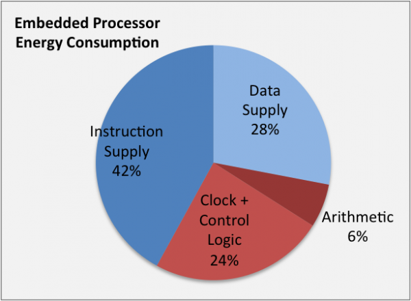
https://www.cast-inc.com/blog/consider-code-density-when-choosing-embedded-processors Quote:
Code Densityâs Effect On Power Consumption
A denser instruction set yields smaller code, which in turn requires fewer instruction fetches. This has a major impact on efficiency, because the energy used to fetch an instruction from on-chip memory is much greater than that required for the CPU to execute that instruction.
How much greater? The 2010 Stanford dissertation study by James Balfour on Efficient Embedded Computing showed that for a typical 32-bit RISC processor, an instruction fetch from a 2 Kbyte on-chip cache consumes 6.8 times more energy than a 32-bit add operation (in a typical 45nm CMOS process).
Another study by Dally et al published in IEEE Computer found that 42% of a typical embedded processorâs energy consumption comes from instruction fetching, and only 6% is consumed by performing the actual arithmetic operations.
Both these studies used a small, on-chip cache. When instructions more realistically need to be accessed from larger, on-chip or even worse off-chip memory, the impact is magnified, and the factor of 6.8x can go to 50x or more.
The conclusion here is clear: using an ISA that requires fewer instructions is a much bigger energy saver than simply selecting a processor that executes more efficiently.
|
The average instruction length of 68k code is less than 3 bytes with some code closer to 2.5 bytes. Instruction fetch of the decoupled instruction fetch pipeline (IFP) continues to fill the instruction buffer as the operand execution pipelines (OEPs) execute instructions with multi-cycle latency, a single instruction that can not superscalar issue and during stalls, most commonly from a cache miss. I know it is difficult for you to comprehend that the unprecedented for a superscalar CPU 68060 4B/cycle instruction fetch can feed such a powerful CPU with minimal lost cycles, but it is true. With other performance improvements and more modern memory bandwidth would it be worthwhile to upgrade to an 8B/cycle instruction fetch? Sure. An 8B/cycle instruction fetch would feed 3 OEPs better than a 4B/cycle instruction fetch feeds two OEPs.
Hammer Quote:
Per clock, there is a certain situation when 68060 is slower than 68040 while Pentium is faster than the 486DX in all situations.
|
The 68040 made everything bigger and wider compared to the 68030 but also increased power and heat. The 68060 design used finesse instead of another brute force upgrade mistake with the result of the 68060 being more successful in the embedded market than the Pentium. In some ways, the 68060 is more like a superscalar 68030 than a 68040. Have you not complained about the 68040 being too expensive and not clocking up enough because of the heat? Was the 68060 not cheaper, lower power/heat with a deeper pipeline for clocking up and with enough area savings to double the caches for the 68060+?
Hammer Quote:
On fictional reborn 68060, X86 side wouldn't be P5 Pentium, it would be various E-Cores X86 uarchs.
The original 68060 designers were keen on doubling the fetch to 8 bytes per cycle fetch rates and they have good reason for fixing this low hanging fruit.
Intel has updated the Pentium class CPU with the Atom Bonnell uarch.
|
Bonnell and Larrabee were both failed Intel attempts to return to the lower power in-order P5 like design. This left them with little choice but to use larger area and increased power OoO cores for their E-Cores which increases costs and limits x86-64 from scaling down into embedded and smart phone markets. ARM E-Cores are in-order and the 68060 demonstrates that the x86(-64) in-order problem is a x86(-64) problem not a CISC problem.
Hammer Quote:
For Quake, the Pentium FDIV situation has out-of-order processing feature that allows other instructions to be processed. Pentium FXCH (zero cycle) can run in parallel with FP operations. Quake made use of these features.
FDIV is used for perspective correction in textures. Texture lookup and filtering processing are done in fixed point integers.
Quake engine is licensed to other game developers, hence its impact goes beyond a single game. FDIV instruction is important for 3D.
Cyrix 6x86 with 3D accelerator didn't solve its FPU problem.
|
The 68060 FPU FDIV can execute in parallel with integer code too. Even the fully pipelined Pentium does not have a pipelined FDIV. The Pentium has optimizations for single and double precision FDIV giving better lantencies than the 68060 extended precision only FDIV but as I recall, the 68060 has better latencies than the Cyrix 6x86 and not just for FDIV. A 68060@75MHz with Voodoo 3-5 on a very low bandwidth Mediator/ZorroIII bus can play GLQuake in 512x384x16-bit at 25fps which looks good and is more than playable. The 68060 was earlier than the Cyrix 6x86 and would have been better overall performance than the Cyrix 6x86 had the 68060 8-stage pipeline advantage been utilized to clock it up to ~150MHz, roughly inline with other deeply pipelined CPUs at that time. The Cyrix 6x86 in-order design is good and perhaps copied from the 68060 but handicapped by the x86 ISA. It is too bad it was not brought back for Vortex86 CPU cores instead of the scalar Cyrix 5x86 but maybe lower power was more important for embedded use which the 68060 architects realized with a more balanced PPA design that still outperformed the Cyrix 6x86 (and P5 Pentium) due to the better 68k ISA.
Heimdall Quote:
I had no idea Pentium's design was so inferior ! I really only cared about the first gen of Pentium, anyway.
|
Intel wanted an efficient in-order Pentium design. The 1997 P55C Pentium MMX came out after the higher performance 1995 OoO P6 Pentium Pro. The in-order P55C was cheaper and the smaller area left room for MMX and doubling the caches, the latter of which was likely the plan for the 68060+ with the 68060 area being smaller than even the first P5 Pentium. Moore's Law soon allowed MMX and doubling the caches for the P6 microarchitecture which was released later in 1997 for the Pentium II but was now up to 7.5 million transistors compared to the P55C 4.5 million transistors and 68060 2.5 million transistors (doubling the 68060 caches would have used a minimum of 786,432 transistors for 16kiB of SRAM but more associative ways would have increased the transistors used).
Heimdall Quote:
That's just awful that 060 was so fast, yet it didn't matter in the end (that's a whole different conversation, though)
|
The 68060 was clearly sabotaged by Motorola. The 68060@66MHz was announced as months away along with plans for the 68060+ and an 8-stage 68060@50MHz was all that ever appeared in Motorola/Freescale information for the full MMU+FPU CPU even though LC and EC versions had higher clock ratings and die shrunk rev 6 68060@50MHz CPUs can often clock over 100MHz. The 68060 was still successful in the embedded market but would have been more successful in the embedded market had it been clocked up as the full static design allows for any clock speed from zero up to max, price efficiency is improved (performance/$) and overall performance is improved. It is a tragedy to design such a great and efficient CPU core and then sabotage it leaving 68k users to use horribly wasteful emulation today instead.
Last edited by matthey on 03-Mar-2025 at 06:25 PM.
|
| | Status: Offline |
| | Hammer
| |
Re: Market Size For New Games requiring 68040+ (060, 080)
Posted on 4-Mar-2025 0:55:28
| | [ #130 ] |
| |
|
Elite Member
|
Joined: 9-Mar-2003
Posts: 6505
From: Australia | | |
|
| @matthey
Quote:
The 68060 4B/cycle fetch does factor in streaming workloads! More memory bandwidth is available for data cache loads and streaming data. Code density makes the small instruction fetch possible which not only saves memory bandwidth but also power.
|
Both 68060 and AC68080 have dual ALU/AGU pipelines with a significant L1 instruction fetch bandwidth difference i.e. 16 bytes per cycle vs 4 bytes per cycle.
For pure scalar integer workload, AC68080's quad decode rate is limited by two ALU/AGU pipelines and it shows AC68080 V2 is superior when compared to 68060 rev6.
For dual ALU/AGU pipelines 68K uarchs at the same clock speed, 68060 rev6 is not delivering AC68080 level performance. AC68080 is faster for wider use cases.
Star Wars Dark Forces port for Amiga 68K
https://eab.abime.net/showpost.php?p=1676594&postcount=398
The fps counter feels like like 060 scaled down to 40 MHz. Which is quite likely, I saw a Sysinfo result of 040/50MHz and it was circa 39 MIPS, as is 060 at the same freq.
What's your result on Trinity 040. please?
68060's 4 byte per cycle fetch from L1 instruction cache. AC68080 has addressed this low hanging fruit.
The TDP problem is a cooling solution problem and the Amigas are not laptops.
Quote:
The 68040 made everything bigger and wider compared to the 68030 but also increased power and heat. The 68060 design used finesse instead of another brute force upgrade mistake with the result of the 68060 being more successful in the embedded market than the Pentium.
|
1. 68060B R&D is cancelled.
2. 68000/68020/CPU32's sales didn't translate into 68060. For embedded AI boom, 68060 is missing in action. MIPS64 CPU family is receiving upgrades e.g. Mobileye EyeQ 6H SoC has MIPS I6500 CPU cores with MIPS Release 6 ISA.
Note that MIPS CPU family gained 16bit instruction set in 1996,
MIPS16 is an Application-Specific Extension for MIPS I through to V designed by LSI Logic and MIPS Technologies, announced on October 21, 1996, alongside its first implementation, the LSI Logic TinyRISC processor. MIPS16 was subsequently licensed by NEC Electronics, Philips Semiconductors, and Toshiba (among others); and implemented as an extension to the MIPS I, II, an III architectures. MIPS16 decreases the size of application by up to 40% by using 16-bit instructions instead of 32-bit instructions
MIPS Inc and LSI Logic encountered critics (resistance), and they adapt i.e. assimilate 16bit instruction set feature.
Release 6 ISA replaced MIPS16 (1996) with microMIPS (2009).
ARM is not the only RISC CPU family that regains variable instruction set length i.e. 16bit Thumb.
MIPS I6500 (2017) basic layout
Quad instruction issue per cycle from L1 instruction cache i.e.
V Pipe 0,
V Pipe 1,
V Pipe 2,
V Pipe 3.
These four V pipes has decode / map dependency check.
Instruction issue unit has five instructions feed into the following pipelines;
Pipe 0: ALU-0 / CTU,
Pipe 1: MDU,
Pipe 2: FPU / MSA (SIMD) Pipe A,
Pipe 3: FPU / MSA (SIMD) Pipe B,
Pipe 4: ALU-1 / LSU (Load-Store Unit),
There's an AGU unit.
MSA = MIPS SIMD Architecture with 128-bit size, reminiscent with 128-bit SSEx (including dual IEEE FP64 and quad IEEE FP32 pack math). 128-bit SIMD registers shares with 64-bit FPU registers. 128bit MSA supports INT8(16 elements), INT16 (8 elements), INT32 (4 elements) and INT64 (2 elements) pack math.
The I6500 core can issue up to two instructions per cycle to the FPU. The FPU contains two execution pipelines for SIMD instruction execution. FPU pipelines doesn't stall when integer pipelines stalls.
For running desktop class PMMU Linux, I6500's TLB cache is relatively large e.g. Fixed TLB (FTLB) cache has dual 512 entries.
MIPS I6500 is a cluster of five CPU cores which shares L2 cache (scales from 256K to 8 MB). MIPS I6500 whitepaper cited cache coherent I/O support. MIPS I6500 cluster can scale with two cluster with a Network on Chip (NOC) block.
AMD Zen 2's dual four CPU CCX cluster with a NB block is not unique. For PS5, Sony selects Zen 2 with 256-bit AVX2 SIMD.
Without factoring AC68080's R&D, the R&D development for Freescale/NXP's 68K family is dead.
Solution for high performance embedded deep learning (AI) SoC would require near desktop level performance.
Smart phones and high-performance embedded deep learning SoCs have seperated themselves from low-performance embedded.
Quote:
In some ways, the 68060 is more like a superscalar 68030 than a 68040. Have you not complained about the 68040 being too expensive and not clocking up enough because of the heat?
|
I wouldn't complain since I know what's needed to be done e.g. I attached a temporary classic Pentium cooler on my 68060 rev1 overclock.
Before PiStorm, I also dismantled a PC cooler with copper heat pipes. PC's aluminum cooling block is relatively easy to cut down to size i.e. they are not iron or steel. I have done metal works subjects during high school. You can attached heatpipes to A1200's RF metal shield.
I have bought some cheap GTX 1660 Ti coolers from Ali Express and cut them to size.
Quote:
Was the 68060 not cheaper, lower power/heat with a deeper pipeline for clocking up and with enough area savings to double the caches for the 68060+?
|
Warp1260 comes with an integrated wedge heatsink and laptop blower fan.
CS Labs understands the desktop gaming audience applied for retro gaming i.e. performance 1st (e.g. 100Mhz 68060) and a cooling solution follows.
Quote:
The 68060 FPU FDIV can execute in parallel with integer code too. Even the fully pipelined Pentium does not have a pipelined FDIV.
|
68060's FDIV is slower e.g. 37 to 39 cycles. https://www.nxp.com/docs/en/data-sheet/MC68060UM.pdf
For instruction size, 6 bytes for longword / 32-bit instructions. http://www.sizecoding.org/wiki/Motorola_68000
This low hanging fruit issue has been solved by AC68080.
Last edited by Hammer on 04-Mar-2025 at 03:11 AM.
Last edited by Hammer on 04-Mar-2025 at 03:08 AM.
Last edited by Hammer on 04-Mar-2025 at 03:03 AM.
Last edited by Hammer on 04-Mar-2025 at 02:34 AM.
Last edited by Hammer on 04-Mar-2025 at 02:30 AM.
Last edited by Hammer on 04-Mar-2025 at 12:59 AM.
_________________
Amiga 1200 (rev 1D1, KS 3.2, PiStorm32/RPi CM4/Emu68)
Amiga 500 (rev 6A, ECS, KS 3.2, PiStorm/RPi 4B/Emu68)
Ryzen 9 7950X, DDR5-6000 64 GB RAM, GeForce RTX 4080 16 GB |
| | Status: Offline |
| | Karlos
| |
Re: Market Size For New Games requiring 68040+ (060, 080)
Posted on 4-Mar-2025 12:47:04
| | [ #131 ] |
| |
 |
Elite Member
|
Joined: 24-Aug-2003
Posts: 4959
From: As-sassin-aaate! As-sassin-aaate! Ooh! We forgot the ammunition! | | |
|
| @Hammer
FDIV ?
The only time you should be using floating point division is if there's no alternative and an angry person has a gun to your head. As soon as more than one number needs to be divided by the same divisor, it should be converted into it's reciprocal so that you can multiply it instead. _________________
Doing stupid things for fun... |
| | Status: Offline |
| | matthey
| |
Re: Market Size For New Games requiring 68040+ (060, 080)
Posted on 4-Mar-2025 23:36:50
| | [ #132 ] |
| |
|
Elite Member
|
Joined: 14-Mar-2007
Posts: 2754
From: Kansas | | |
|
| Hammer Quote:
Both 68060 and AC68080 have dual ALU/AGU pipelines with a significant L1 instruction fetch bandwidth difference i.e. 16 bytes per cycle vs 4 bytes per cycle.
For pure scalar integer workload, AC68080's quad decode rate is limited by two ALU/AGU pipelines and it shows AC68080 V2 is superior when compared to 68060 rev6.
|
Do I need to explain to you again how a decoupled instruction fetch pipeline and instruction buffer works and why it reduces instruction fetch requirements or would you just ignore me again?
Hammer Quote:
For dual ALU/AGU pipelines 68K uarchs at the same clock speed, 68060 rev6 is not delivering AC68080 level performance. AC68080 is faster for wider use cases.
|
The AC68080 is a 64-bit CPU core and the 68060 uses a 32-bit CPU core. The AC68080 design target is max performance at the expense of power since area is already heavily constrained by the affordable FPGA size compared to even a small ASIC.
Hammer Quote:
Star Wars Dark Forces port for Amiga 68K
https://eab.abime.net/showpost.php?p=1676594&postcount=398
The fps counter feels like like 060 scaled down to 40 MHz. Which is quite likely, I saw a Sysinfo result of 040/50MHz and it was circa 39 MIPS, as is 060 at the same freq.
What's your result on Trinity 040. please?
68060's 4 byte per cycle fetch from L1 instruction cache. AC68080 has addressed this low hanging fruit.
The TDP problem is a cooling solution problem and the Amigas are not laptops.
|
The 68060 shares resources between the integer OEPs so sometimes there are fewer resources available than the single integer 68040 execution pipeline. The 68060 design is a balanced PPA design, was a successful embedded design and the design could have been used in laptops. The 68060 was not a max performance desktop design although the deep 8-stage pipeline for high clock speeds and small area with room to double the caches a la 68060+ opened up the possibility for easily increasing the performance, Motorola decided to AIM for PPC instead.
Hammer Quote:
1. 68060B R&D is cancelled.
2. 68000/68020/CPU32's sales didn't translate into 68060. For embedded AI boom, 68060 is missing in action. MIPS64 CPU family is receiving upgrades e.g. Mobileye EyeQ 6H SoC has MIPS I6500 CPU cores with MIPS Release 6 ISA.
|
With no 68k future plans and no product pipeline, embedded developers only used the 68k for small projects and for short lived products although this was still enough to keep the 68k the #1 32-bit embedded CPU by volume for another decade or so. Eventually, the silicon was too much of a handicap and SoCs and MCUs were too much of an advantage to keep using old 68k and later ColdFire CPUs. The 68k was much loved for its ease of programming and industry leading code density but ARM eventually came close enough with Thumb ISAs. PPC died much quicker than the 68k once it was no longer supported.
Where in time is Hammer meandering? Do you mean the first AI boom with fuzzy logic or the more recent AI bubble that seems to be deflating?
Hammer Quote:
Note that MIPS CPU family gained 16bit instruction set in 1996,
MIPS16 is an Application-Specific Extension for MIPS I through to V designed by LSI Logic and MIPS Technologies, announced on October 21, 1996, alongside its first implementation, the LSI Logic TinyRISC processor. MIPS16 was subsequently licensed by NEC Electronics, Philips Semiconductors, and Toshiba (among others); and implemented as an extension to the MIPS I, II, an III architectures. MIPS16 decreases the size of application by up to 40% by using 16-bit instructions instead of 32-bit instructions
MIPS Inc and LSI Logic encountered critics (resistance), and they adapt i.e. assimilate 16bit instruction set feature.
Release 6 ISA replaced MIPS16 (1996) with microMIPS (2009).
ARM is not the only RISC CPU family that regains variable instruction set length i.e. 16bit Thumb.
|
The compressed MIPS16 ISA was so good that it was replaced by the compressed microMIPS ISA. It was replaced because MIPS16 requires a pipeline flushing mode switch to use the 32-bit instruction encodings like ARM Thumb. MIPS16 is a copy of Thumb and microMIPS is a copy of Thumb-2.
1994 Thumb
1996 MIPS16
2003 Thumb-2
2009 microMIPS
The problem was the inferior copy of the variable length encoded 68k ISA to the fixed length 16-bit encoding of SuperH which was licensed to ARM for Thumb. This was RISC lemmings playing follow the leader instead of doing the research to look at the original 68k technology which of course was bad because it was "CISC". It is better to start with a variable length encoded ISA rather than add it. RISC-V finally got that part right although it still falls well short of the 68k VLE in performance and code density. Even the Thumb-2 add-on easily beats RISC-V code density.
Hammer Quote:
The 68060 FPU latency is better than the Pentium FPU latency for an extended precision FDIV.
FPU latencies in cycles
FPU | fdiv.s | fdiv.d | fdiv.x
68060 37 37 37
Pentium 19 33 39
The 68060 has 8 FPU registers and the Pentium FPU stack ISA is closer to 1 FPU register. The 68060 FDIV can access memory with no added latency while the Pentium requires 3 additional cycles. The 68060 can issue an integer instruction in parallel while the Pentium can only issue a FXCH instruction in parallel in order to have access to more than one stack register. Additional integer instructions can issue and execute in parallel in subsequent code until FDIV completion unless another FPU instruction is encountered as neither the Pentium or the 68060 have a fully pipelined FDIV unit. The Pentium single precision FDIV has a large latency advantage but switching the precision requires a FLDCW instruction with 8 cycle latency, unless single precision is adequate all the time. Once again, the Pentium may have better performance in narrow use cases with hand optimized assembly code but I expect it disappears when using a compiler.
Karlos Quote:
FDIV ?
The only time you should be using floating point division is if there's no alternative and an angry person has a gun to your head. As soon as more than one number needs to be divided by the same divisor, it should be converted into it's reciprocal so that you can multiply it instead.
|
Yet, FPUs still have hardware FDIV and FSQRT units with FSQRT even less commonly used. Even the stripped down 68040 and 68060 FPU kept hardware FDIV and FSQRT though.
Even the assembler VASM peephole optimizer for the 68k can perform the invert and multiply trick along with compress the immediate where there is no loss of precision (FPCC is the same).
http://sun.hasenbraten.de/vasm/release/vasm.pdf Quote:
-opt-fconst
Floating point constants are loaded with the lowest precision possible. This means that FMOVE.D #1.0,FP0 would be optimized to FMOVE.S #1.0,FP0, or even FMOVE.W #1,FP0, because it is faster and shorter at the same precision. The optimization will be performed on all FPU instructions with immediate addressing mode. When an FDIV-family instruction (FSDIV, FDDIV, FSGLDIV) is detected it will additionally be checked if the immediate constant is a power of 2 and then converted into FMUL #1/c,FPn.
|
I hope Frank did not add the FMOVE.W optimization except when compiling for size and maybe for targets like the AC68080 where integer to fp conversion is free. Similar immediate compression could be achieved if half precision float was supported although Gunnar did not like the idea. It would also be possible to enable an option where some level of precision loss was acceptable. GCC has similar options from early versions but oddly not either of the "-opt-fconst" peephole optimizations VASM performs. I wonder how much this optimization had to do with the VBCC compiled fp ByteMark benchmark on a 68060@50MHz having more than twice the performance of a GCC 3.3 compiled fp Bytemark on a 68060@75MHz and how much was my VBCC support code changes. Removing trapped FPU instructions is good for performance too. Too bad VBCC will never get an improved integer 68k backend with emulation negating the need for performance improvements and optimizations but EOL is EOL. There will be no 68060 Quake beating the Pentium without a better VBCC 68k integer backend and we will have to listen to Hammer complain about it endlessly.
Last edited by matthey on 04-Mar-2025 at 11:49 PM.
|
| | Status: Offline |
| | Hammer
| |
Re: Market Size For New Games requiring 68040+ (060, 080)
Posted on 5-Mar-2025 0:29:49
| | [ #133 ] |
| |
|
Elite Member
|
Joined: 9-Mar-2003
Posts: 6505
From: Australia | | |
|
| @Karlos
Quote:
Karlos wrote:
@Hammer
FDIV ?
The only time you should be using floating point division is if there's no alternative and an angry person has a gun to your head. As soon as more than one number needs to be divided by the same divisor, it should be converted into it's reciprocal so that you can multiply it instead. |
Are you defending reborn 68060 fiction?
Other instructions have their clock cycle completion times.
68060
FPU is not pipelined.
FMUL has 3 to 5 clock cycles.
FADD has 3 to 5 clock cycles.
Pentium
FPU is pipelined.
FMUL has 3 cycles
FADD has 3 cycles
At a given process node, Pentium can reach higher clock speeds. Pipeline stage count is not the only factor for attainable clock speed e.g. circuit layout's craftsmanship can influence reachable clock speed. This is why X86 and ARM assimilated DEC Alpha engineers' skills.
Star Wars Dark Forces (The Force engine) port for Amiga 68K has tripped 68060's 4 bytes per cycle instruction cache fetch rate limit.
The Force engine is designed for modern CPUs and the 68060 is shown to be not modern.
A reborn 68060 will face modernized CPU core competition at the current time, that can run full Linux with beefy MMU TLB cache.Last edited by Hammer on 05-Mar-2025 at 04:12 AM.
_________________
Amiga 1200 (rev 1D1, KS 3.2, PiStorm32/RPi CM4/Emu68)
Amiga 500 (rev 6A, ECS, KS 3.2, PiStorm/RPi 4B/Emu68)
Ryzen 9 7950X, DDR5-6000 64 GB RAM, GeForce RTX 4080 16 GB |
| | Status: Offline |
| | Hammer
| |
Re: Market Size For New Games requiring 68040+ (060, 080)
Posted on 5-Mar-2025 2:51:19
| | [ #134 ] |
| |
|
Elite Member
|
Joined: 9-Mar-2003
Posts: 6505
From: Australia | | |
|
| @matthey
Quote:
Do I need to explain to you again how a decoupled instruction fetch pipeline and instruction buffer works and why it reduces instruction fetch requirements or would you just ignore me again?
|
For Star Wars Dark Forces, The Force Engine Amiga 68K port gimped your 68060 into effective high clock speed 68040.
The Force Engine is designed for modern CPUs and its results show 68060 needs a sizable modernization.
Your "decoupled instruction fetch pipeline" argument doesn't factor in slow entry point i.e. a pipeline is only as good as the entry point.
68060's narrow 4 bytes per cycle instructions entry point is just bad as Pentium IV's single X86 complex decoder.
Pentium IV has one X86 complex hardware decoder + one microcode decoder. This design mistake was thrown in the bin.
Quote:
The AC68080 is a 64-bit CPU core and the 68060 uses a 32-bit CPU core. The AC68080 design target is max performance at the expense of power since area is already heavily constrained by the affordable FPGA size compared to even a small ASIC.
|
Apollo-Computer is a very small company and their mainline FPGA usage is SoC, which includes more than just firmware CPU softcore. Apollo-Computer relies on the effort from Intel's Cyclone V platform. Money doesn't grow on trees and this is a business development plan issue.
Quote:
With no 68k future plans and no product pipeline, embedded developers only used the 68k for small projects and for short lived products although this was still enough to keep the 68k the #1 32-bit embedded CPU by volume for another decade or so. Eventually, the silicon was too much of a handicap and SoCs and MCUs were too much of an advantage to keep using old 68k and later ColdFire CPUs. The 68k was much loved for its ease of programming and industry leading code density but ARM eventually came close enough with Thumb ISAs. PPC died much quicker than the 68k once it was no longer supported.
|
The writing is on the wall with ColdFire V's single major design win, i.e. HP's enterprise printers.
My Japanese branded color laser printer has non-Book E PowerPC instead.
Quote:
Where in time is Hammer meandering? Do you mean the first AI boom with fuzzy logic or the more recent AI bubble that seems to be deflating?
|
For lower tier CPU families, embedded AI is aiding the demand factor to push these embedded CPUs to evolve.
AI bubble is against costly NVIDIA's AI solutions. NVIDIA still has raytracing as a bottomless pit for increasing compute power.
Both smartphones and the embedded AI market demand are pushing non-x86 instruction set CPU families into a higher level of performance, and they have a sizable amount of customers buying them.
Quote:
The 68060 FPU latency is better than the Pentium FPU latency for an extended precision FDIV.
FPU latencies in cycles
FPU | fdiv.s | fdiv.d | fdiv.x
68060 37 37 37
Pentium 19 33 39
|
Quake FDIV uses FP32. Quake 2's 3DNow path used FP32.
Real world embedded Zen 2 e.g. PS5/PS5 Pro, Xbox SX/SS, SteamDeck, latencies in cycles
X87 FDIV(R)(P) = 15,
XMM/YMM
DIVSS = 3 (scalar divide for FP32)
DIVPS = 3 (vector divide for FP32)
DIVSD = 5 (scalar divide for FP64)
DIVPD = 5 (vector divide for FP64)
MULSS = 3 (scalar MUL for FP32)
MULSD = 3 (scalar MUL for FP64)
AMD Bobcat in tablet form factor with dual X86 instruction decodes per cycle E-Core
X87
FMUL(P) = 5
FDIV(R)(P) = 19
FDIV(R)(P) = 19
XMM FP
MULSS = 2 (scalar MUL for FP32)
MULSD = 4 (scalar MUL for FP64)
MULPS = 2 (vector MUL for FP32)
MULPD = 4 (vector MUL for FP64)
DIVSS = 13 (scalar divide for FP32)
DIVPS = 38 (vector divide for FP32)
DIVSD = 19 (scalar divide for FP64)
DIVPD = 34 (vector divide for FP64)
AMD Jaguar, embedded game consoles such as PS4 and Xbox One, with dual X86 instruction decodes per cycle E-Core.
X87
FMUL(P) = 5
FDIV(R)(P) = 22
XMM FP
MULSS = 2 (scalar MUL for FP32)
MULPS = 2 (vector MUL for FP32)
MULSD = 4 (scalar MUL for FP64)
MULPD = 4 (vector MUL for FP64)
DIVSS = 14 (scalar divide for FP32)
DIVPS = 19 (vector divide for FP32)
DIVSD = 19 (scalar divide for FP64)
DIVPD = 19 (vector divide for FP64)
Real-world embedded PS4 and Xbox One game console has AMD's Jaguar E-Cores.
Pentium MMX, no design wins for embedded game consoles.
X87
FDIV(R)(P) = 19/33/39 (FP32, FP64 and FP80 respectively)
FMUL(P) = 3
FIMUL = 6 (integer MUL on FPU)
Pentium III via Coppermine 128K with design win for embedded Xbox game console.
X87
FDIV(R)(P) = 18 for FP32, 32 for FP64, 38 for FP80,
FMUL(P) r = 5
FMUL(P) m = 5 to 6
Applicable for Pentium II
XMM
MULSS = 4 (scalar MUL for FP32)
MULPS = 4 (vector MUL for FP32)
DIVSS = 18 (scalar divide for FP32)
DIVPS = 48 (vector divide for FP32), effectively 12 cycles per 32bit value A/ 32bit value B divide operations.
K7 Athlon, aborted K7 Duron original Xbox alternative. Bill Gates overrides K7 Duron Xbox over Xbox team's selection.
X87
FMUL(P) = 4
FDIV(R)(P) = 11-25
3DNow
PFMUL = 4 (vector MUL for FP32)
PFRSQRT = 3 (vector sq root)
PFRSQIT1 = 4 (vector reciprocal square root approximation)
XMM (later steppings)
MULSS = 4 (scalar MUL for FP32)
MULPS = 4 (vector MUL for FP32)
DIVSS = 11-16 (scalar divide for FP32)
DIVPS = 18-30 (vector divide for FP32)
Quake FP uses up to FP32.
Quote:
The 68060 has 8 FPU registers and the Pentium FPU stack ISA is closer to 1 FPU register.
|
FALSE, Pentium's zero cycle FXCH effectively makes X87 registers into 8 x87 registers.
Both the Pentium FPU and the 68060 FPU are attached to one of the integer pipelines and both CPU families don't have FMA3 instructions. Your "68060 has 8 FPU registers" argument is useless.
68060 is not PowerPC 601 FPU. Ex-original Amiga engineers in 3DO didn't pick 68060 for M2 since they selected PPC 602 with 32 register FP32/FMA3 FPU. PA-RISC 7150 FPU is very strong.
Your argument would be valid when 68060 has multiple entry ports for concurrent floating point operations.
Real world embedded X86 based game consoles have at least SSE.
X86 evolved into separated FADD and FMUL pipelines, and later gained FMA3 with FMUL pipelines.
--------------------------
The initial BOM costings for the original Xbox
https://www.neogaf.com/threads/3do-mx-chipset-the-technology-nintendo-almost-used-in-an-n64-successor-for-1999.350196/#post-14521193
Brown said the goals were to make money, expand Microsoft's technology into the living room, and create the perception that Microsoft was leading the
charge in the new era of consumer appliances. The initial cost estimate was for a machine with a bill of materials (engineering talk for cost) of $303. That
machine would debut in the fall of 2000 and use a $20 microprocessor running at 350 megahertz from Advanced Micro Devices. The machine would also have
a $55 hard disk drive with two gigabytes of storage, a $27 DVD drive to play movies, a $35 graphics chip, $25 worth of memory chips, and a collection of
other standard parts like a motherboard, and power supply. Over time, these prices would decline.
$20 Intel-compatible microprocessor and a $30 graphics chip from Nvidia. The highest-priced item on the list of materials was $40 for memory chips. But the
rest of the bill of materials was complete, down to $2.14 for the cables and $4.85 for screws
Xbox's BOM cost parameters are close to mainstream Amiga AGA (e.g. A1200), Amiga Hombre (proposed CD32 game console successor) and 3DO.
Motorola couldn't match X86 vendor's CPU performance vs price offer for Xbox project.
Intel has bid for Sony PS6 and MS Xbox Next 2028 high-performance embedded game console contracts and lost.
Around 1987, SGI complains about Motorola's 68030's performance vs price.
Quote:
The 68060 FDIV can access memory with no added latency while the Pentium requires 3 additional cycles. The 68060 can issue an integer instruction in parallel while the Pentium can only issue a FXCH instruction in parallel in order to have access to more than one stack register.
|
There will be latency exceeding 68060's external 32bit bus.
Per clock cycle, 68060 still lost Quake benchmark to P5 Pentium.
Pipelining helps with hiding latency and Pentium FPU is pipelined.
Quote:
Additional integer instructions can issue and execute in parallel in subsequent code until FDIV completion unless another FPU instruction is encountered as neither the Pentium or the 68060 have a fully pipelined FDIV unit.
|
Pentium's FPU is pipelined. Encountering FDIV only stalls new FP operations.
Quote:
The Pentium single precision FDIV has a large latency advantage but switching the precision requires a FLDCW instruction with 8 cycle latency, unless single precision is adequate all the time. Once again, the Pentium may have better performance in narrow use cases with hand optimized assembly code but I expect it disappears when using a compiler.
|
Per clock cycle, 68060 still lost Quake benchmark to P5 Pentium.
Quake engine is licensed to multiple 3rd party game developers, hence its impact is not limited to a single game.
FP32 dominates modern 3D gaming.
AMD FSR4 AI use FP8 format in Radeon RX 9070 series, which is missing in Radeon RX 7000 series.
----------
Star Wars Dark Forces doesn't require a FPU, hence its integer-based game engine, and it wasn't a good showing on 68060's integer superscalar against 50Mhz 68040.
GE has 60 Mhz 68040 in the Model 2907C1 product and why not 68060?
Last edited by Hammer on 05-Mar-2025 at 04:29 AM.
Last edited by Hammer on 05-Mar-2025 at 04:11 AM.
Last edited by Hammer on 05-Mar-2025 at 03:20 AM.
Last edited by Hammer on 05-Mar-2025 at 02:58 AM.
_________________
Amiga 1200 (rev 1D1, KS 3.2, PiStorm32/RPi CM4/Emu68)
Amiga 500 (rev 6A, ECS, KS 3.2, PiStorm/RPi 4B/Emu68)
Ryzen 9 7950X, DDR5-6000 64 GB RAM, GeForce RTX 4080 16 GB |
| | Status: Offline |
| | Karlos
| |
Re: Market Size For New Games requiring 68040+ (060, 080)
Posted on 5-Mar-2025 17:50:52
| | [ #135 ] |
| |
|
Elite Member
|
Joined: 24-Aug-2003
Posts: 4959
From: As-sassin-aaate! As-sassin-aaate! Ooh! We forgot the ammunition! | | |
|
| @Hammer
Re: fdiv Do you even understand what I wrote?
If you are going to divide more than one number by some divisor x, it's almost always faster to first convert x into 1.0/x and then multiply the other numbers by this. Multiplication is almost always faster than division on every architecture going that supports both operations. You'll typically save cycles by the time you are dividing two successive numbers by x and it just gains from there.
The point being, fdiv is a pretty lousy argument point because almost anyone writing performant code will be avoiding it as much as humanly possible.
_________________
Doing stupid things for fun... |
| | Status: Offline |
| | bhabbott
| |
Re: Market Size For New Games requiring 68040+ (060, 080)
Posted on 5-Mar-2025 22:55:20
| | [ #136 ] |
| |
 |
Cult Member
 |
Joined: 6-Jun-2018
Posts: 554
From: Aotearoa | | |
|
| @Hammer
Quote:
Hammer wrote:
Tomb Raider is available as open source via the OpenLara project and it was ported to 3DO. |
So it shouldn't be hard to port to the Amiga, right? Who's up for it?
Quote:
| AC68080 exists as one of the major 68K solutions for the Amiga |
...and is faster than an 80MHz 060, so it should have plenty enough grunt for Tomb Raider.
Quote:
| For pure scalar integer workload, AC68080's quad decode rate is limited by two ALU/AGU pipelines and it shows AC68080 V2 is superior when compared to 68060 rev6. |
Sweet! I can almost smell that Tomb Raider port now!
Quote:
| I attached a temporary classic Pentium cooler on my 68060 rev1 overclock. |
I attached a CPU cooling fan to the 68060 in my A3000 and it was a pain because I had to cut a hole in the drive stage. That steel was thick! (no wonder the A3000 weighed so much). Even so, I couldn't clock the CPU over 64MHz without it getting flaky, barely enough to make Quake playable. Wish I had known about those 75MHz Rev 6 chips.
In comparison, the FPGA in my V2 Vampire runs cool enough that it doesn't need a fan in my A600. That's more than I can say for the 68020 I used to run in it.
I agree that the 68080 is a major 68K solution for the Amiga. You get a faster 68k than any 68060, that runs cooler and costs less than a full 060, with decent RTG. I don't see a need for any more than this. OTOH, Pistorm delivers a cheaper solution that is in many cases faster (though not as compatible) and has the advantage of being open source. These two solutions make developing a 'reborn' 68060 pointless. Better to concentrate on getting more out of what we have.
Quote:
| The Force Engine is designed for modern CPUs and its results show 68060 needs a sizable modernization. |
No, it shows that we need engines designed for the 68060.
Quote:
| FDIV is used for perspective correction in textures. Texture lookup and filtering processing are done in fixed point integers. |
Karlos says "fdiv is a pretty lousy argument point because almost anyone writing performant code will be avoiding it as much as humanly possible.". But is that actually happening? I'm no expert on 3D rendering, but I looked at the source code for OpenLara and in the 'transform' routine it had this:-
c.x /= c.w;
c.y /= c.w;
c.z /= c.w;
Is this one of those cases where divide can't be avoided, or the compiler converts it to multiply, or is it just crappy code? If I was porting this code I wouldn't change anything that I didn't understand, which would be 99% of it. And even then it probably wouldn't work. I guess we need a coding expert like Karlos to do the job.
|
| | Status: Offline |
| | OneTimer1
| |
Re: Market Size For New Games requiring 68040+ (060, 080)
Posted on 5-Mar-2025 23:10:55
| | [ #137 ] |
| |
 |
Super Member
 |
Joined: 3-Aug-2015
Posts: 1260
From: Germany | | |
|
| @Thread
I think some people should have their own forum for discussions, instead of turning a thread about the market for a game, into an endless discussion about CPU architecture.
Maybe the admins would install a KI bot opening weekly threads about CPU performance, FPU architectures, shader pipelines, cache technology and their important meaning for a 68k retro platform. Last edited by OneTimer1 on 05-Mar-2025 at 11:11 PM.
|
| | Status: Offline |
| | Karlos
| |
Re: Market Size For New Games requiring 68040+ (060, 080)
Posted on 5-Mar-2025 23:55:27
| | [ #138 ] |
| |
|
Elite Member
|
Joined: 24-Aug-2003
Posts: 4959
From: As-sassin-aaate! As-sassin-aaate! Ooh! We forgot the ammunition! | | |
|
| @bhabbott
Try it. Assign 1.0/c.w to a temporary and then multiply each component by it. I would expect a good compiler to spot this but it may not optimise it because there are potential side effects to care about for strictness where c.w is very large. For most practical transformations, that wouldn't be the case.
This just looks like code written for clarity, rather than performance and the assumption the compiler will just magically fix it.
In this example, you can trade 3 divisions for 1 division and 3 multiplications. Division is typically an order of magnitude slower than multiplication on most FPU. Some FPU might even have a reciprocal operation (1/x) that's quicker than a regular general purpose division (not seen an example, but it's the sort of thing that could conceivably exist).
Maybe I can write a simple proof of concept benchmark for this for 882 and 060, but I'm equally sure you could too. _________________
Doing stupid things for fun... |
| | Status: Offline |
| | Hammer
| |
Re: Market Size For New Games requiring 68040+ (060, 080)
Posted on 6-Mar-2025 1:08:55
| | [ #139 ] |
| |
|
Elite Member
|
Joined: 9-Mar-2003
Posts: 6505
From: Australia | | |
|
| @bhabbott
Quote:
...and is faster than an 80MHz 060, so it should have plenty enough grunt for Tomb Raider. |
Without PiStorm-Emu68, AC68080 V2 would be my next choice. I'm okay with 68080's CPU core design.
The main reason why purchased TF1260 is to investigate the so-called untapped hype with 68060 rev1 since this is the CPU that would be in my A3000/030-25 before I sold it in 1996.
If games wasn't a big factor in 1996, PowerMac would be selected instead.
Quote:
I attached a CPU cooling fan to the 68060 in my A3000 and it was a pain because I had to cut a hole in the drive stage. That steel was thick! (no wonder the A3000 weighed so much). Even so, I couldn't clock the CPU over 64MHz without it getting flaky, barely enough to make Quake playable. Wish I had known about those 75MHz Rev 6 chips.
|
At my university during 1997, Pentium Socket 7 PC clones are in metal box cages while PowerMacs doesn't need them. PC clone cases are cheap soft skin metal.
When my local PC shop was upgrading my A3000's RAM into 4 MB ZIP RAM, he commented on A3000's overkill build construction.
Quote:
No, it shows that we need engines designed for the 68060.
|
Nope. It shows 68060's 4 byte per cycle fetch limit is easily tripped over. This issue is fixed for 68080.
Star Wars Dark Forces doesn't need a FPU.
Other semi-modern embedded CPUs doesn't have 68060's 4 byte per cycle fetch limit.
MIPS64 has gained 16-bit compressed instructions, hence it's so what moment with Matt's 68K code density argument.
_________________
Amiga 1200 (rev 1D1, KS 3.2, PiStorm32/RPi CM4/Emu68)
Amiga 500 (rev 6A, ECS, KS 3.2, PiStorm/RPi 4B/Emu68)
Ryzen 9 7950X, DDR5-6000 64 GB RAM, GeForce RTX 4080 16 GB |
| | Status: Offline |
| | Hammer
| |
Re: Market Size For New Games requiring 68040+ (060, 080)
Posted on 6-Mar-2025 1:35:39
| | [ #140 ] |
| |
|
Elite Member
|
Joined: 9-Mar-2003
Posts: 6505
From: Australia | | |
|
| @Karlos
Quote:
Re: fdiv Do you even understand what I wrote?
If you are going to divide more than one number by some divisor x, it's almost always faster to first convert x into 1.0/x and then multiply the other numbers by this. Multiplication is almost always faster than division on every architecture going that supports both operations. You'll typically save cycles by the time you are dividing two successive numbers by x and it just gains from there.
The point being, fdiv is a pretty lousy argument point because almost anyone writing performant code will be avoiding it as much as humanly possible.
|
The Quake example used FDIV at a certain interval to correct the perspective i.e. every 8 pixels, Quake will use FDIV-based perspective correction. Michael Abrash knows FDIV is costly for P5 Pentium.
Encountering FDIV instruction, Pentium FPU with halt any new x87 instruction processing, hence integer instructions to be interleaved. Pentium FPU is pipelined.
Newer uArch CPUs has multiple FPU pipelines with out of order processing.
Dual issue in-order processing Cortex A53 has two FPU pipelines connected from four ports
https://hardwarebug.org/2014/05/15/cortex-a7-instruction-cycle-timings/
Cortex A7's VFP instructions
VDIV FP32
Issue cycles: 15
Result latency: 18
VDIV FP64
Issue cycles: 29
Result latency: 32
VMUL FP32
Issue cycles: 1
Result latency: 4
NEON SIMD
VMUL F32
Issue cycles: 2
Result latency: 4
Matt's reborn 68060 is in dreamland.
AC68080 is a better candidate for a modern 68K ASIC. AC68080 needs a working MMU for modern PMMU Linux IoT and Trusted Zone hardware would be nice for IoT e.g. embedded casino games with secured payment.
There's a sufficient amount of work for modernizing 68060. Money doesn't grow on trees.
Inverse square root would need FDIV and Quake 3 has a fast inverse square root approximation software workaround, but modern X86 SSE has instructions for inverse square root e.g. RSQRTSS.
AMD Bobcat's RSQRTSS latency is 3 cycles.
AMD Jaguar RSQRTSS latency is 2 cycles.
Pentium III's RSQRTSS latency is 1 to 2.
Atom Silvermont's RSQRTSS latency is 4.
Skylake's RSQRTSS latency is 4.
Pentium M's RSQRTSS latency is 3.
AMD K7's RSQRTSS latency is 3.
Hardware RSQRTSS will beat Quake 3's non-SSE inverse square root approximation software workaround.
Modern X86 CPUs even with E-Core grade are designed for Quake/Quake II/Quake III.
That's a specific ASIC use case to accelerate Quake 3's CPU bottleneck hot spots.
This is getting absurd to think reborn 68060 beating modern game consoles!
Motorola doesn't listen to gamers and they were kickout of games. Apollo-Core is different since they have a bias towards games.
I wonder who still has the original Amiga spirit? It's not Motorola/Freescale/NXP.
Last edited by Hammer on 06-Mar-2025 at 02:46 AM.
Last edited by Hammer on 06-Mar-2025 at 02:09 AM.
Last edited by Hammer on 06-Mar-2025 at 02:00 AM.
Last edited by Hammer on 06-Mar-2025 at 01:56 AM.
Last edited by Hammer on 06-Mar-2025 at 01:39 AM.
Last edited by Hammer on 06-Mar-2025 at 01:37 AM.
_________________
Amiga 1200 (rev 1D1, KS 3.2, PiStorm32/RPi CM4/Emu68)
Amiga 500 (rev 6A, ECS, KS 3.2, PiStorm/RPi 4B/Emu68)
Ryzen 9 7950X, DDR5-6000 64 GB RAM, GeForce RTX 4080 16 GB |
| | Status: Offline |
| |
|
|
|
[ home ][ about us ][ privacy ]
[ forums ][ classifieds ]
[ links ][ news archive ]
[ link to us ][ user account ]
|