Your support is needed and is appreciated as Amigaworld.net is primarily dependent upon the support of its users.

|
|
|
|
| Poster | Thread |  matthey matthey
|  |
Re: The Case for the Complex Instruction Set Computer
Posted on 18-Nov-2023 9:55:39
| | [ #21 ] |
| |
 |
Elite Member
 |
Joined: 14-Mar-2007
Posts: 2052
From: Kansas | | |
|
| cdimauro Quote:
That's why an SMT solutions would have been a perfect fit for the G5.
|
Sure, parallel performance is better than nothing but single core/thread performance is what is needed to compete with CISC.
cdimauro Quote:
How is it possible to generate the address of instructions that aren't decoded and even not yet fetched?
|
I believe its the address calculation of the PC in connection with the branch unit. PC=PC+4 unless branch unit predicts new PC (fetch=4 bytes/cycle).
cdimauro Quote:
You're comparing a 2-ways in-order core to a very aggressive 4-ways OoO core (Intel's Skylake is a beast. AMD's first Zen is more between Intel's Ivy Bridge and Haswell).
You've to compare the 68060 core to the Pentium core, which is more similar to it.
|
The Pentium is not as efficient as the 68060 in executing superscalar instructions because it lacked orthogonality. The 68060 has a high multi-issue percentage. Easy scheduling and good code density reduced stalls. The biggest integer unit limitation was energy, transistor and cost saving small data limitations like a small fetch, 6 byte superscalar instruction limitation and 32 bit data bus. Intel tried to go back to simpler Pentium like in-order core designs with Atom and Larrabee cores but x86-64 large instructions and more complex decoding made it difficult.
cdimauro Quote:
No, the Pentium M still used 118-bit micro-ops. There's another thing of this part of the article which clarifies how those 236-bit are used:
On P6 architecture, each microinstruction is 118-bit long. Pentium M instead of working with 118-bit micro-ops works with 236-bit long micro-ops that are in fact two 118-bit micro-ops.
Keep in mind that the micro-ops continue to be 118-bit long; what changed is that they are transported in groups of two.
So, they are moved around two at the time to make it faster. But micro-ops stay 118-bit long and executed as such by the execution units.
|
If the Pentium M micro-ops are always used in pairs then I would call them 236 bit. Otherwise I would say they are 118 bit. Regardless, it looks like it is possible to use large data representations of single instructions.
cdimauro Quote:
If you compare it to the original 68060 design and even to the x86 designs, yes: it's very radical.
I show you what I've found on the above article (I See Dead µops: Leaking Secrets via Intel/AMD Micro-Op Caches) that you've posted before:
64-bit immediate values consume two micro-op slots within a given cache line.
which matches what I was recalling: instructions handling big values are internally split in two micro-ops. I assume that this was decided to save space on the micro-op cache, by having micro-ops of reduced length.
Which makes sense: take into account the more common cases and use more micro-ops for the less common ones.
That simplicity should be used for a modernized 68060 core.
|
For a micro-op cache in memory, I can see how alignment could be important. For executing macro-ops directly from an instruction buffer, I don't see how alignment is important. This is why the macro-ops are odd sizes too. A 118 bit macro-op is 14.75 bytes.
cdimauro Quote:
IMO those 48 bits only as early decoding information are way too much. I was wondering before when you've first reported it and now I'm even more convinced about it.
If an x86 core can use 118 bits having a maximum instruction length of 15 bytes (which is very artificial: you can reach it only by adding redundant, unused extra prefixes) and performing so well, a modernized 68060 core should move to a similar solution. IMO. |
Perhaps the 68060 macro-op bits could be used more efficiently. SRAM is likely cheaper than more complex logic though.
|
| | Status: Offline |
| | OneTimer1
| |
Re: The Case for the Complex Instruction Set Computer
Posted on 18-Nov-2023 19:21:22
| | [ #22 ] |
| |
 |
Cult Member
 |
Joined: 3-Aug-2015
Posts: 989
From: Unknown | | |
|
| @thread
most computers today are real 'Complex Instruction Set Computer' they can use multiple and complex sets of instructions in their command interfaces, interpreter languages or compilers.
CPU architectures are insignificant, as long as you can get software delivering the complexity needed
Last edited by OneTimer1 on 18-Nov-2023 at 07:22 PM.
|
| | Status: Offline |
| | cdimauro
| |
Re: The Case for the Complex Instruction Set Computer
Posted on 19-Nov-2023 6:49:05
| | [ #23 ] |
| |
 |
Elite Member
|
Joined: 29-Oct-2012
Posts: 3650
From: Germany | | |
|
| @matthey
Quote:
matthey wrote:
cdimauro Quote:
That's why an SMT solutions would have been a perfect fit for the G5.
|
Sure, parallel performance is better than nothing but single core/thread performance is what is needed to compete with CISC. |
Absolutely. Single core/thread performance is my primary reference for any ISA.
Quote:
cdimauro Quote:
You're comparing a 2-ways in-order core to a very aggressive 4-ways OoO core (Intel's Skylake is a beast. AMD's first Zen is more between Intel's Ivy Bridge and Haswell).
You've to compare the 68060 core to the Pentium core, which is more similar to it.
|
The Pentium is not as efficient as the 68060 in executing superscalar instructions because it lacked orthogonality. |
Why? On both the two pipes are specialized and cannot execute the same instructions. They are quite similar from this perspective.
Quote:
| The 68060 has a high multi-issue percentage. Easy scheduling and good code density reduced stalls. The biggest integer unit limitation was energy, transistor and cost saving small data limitations like a small fetch, 6 byte superscalar instruction limitation and 32 bit data bus. |
Whatever, but they have very similar microarchitectures and also from performance perspective.
Why do you insist on not having it as a reference? They were also fighting each other on the same (desktop) market...
Quote:
| Intel tried to go back to simpler Pentium like in-order core designs with Atom and Larrabee cores but x86-64 large instructions and more complex decoding made it difficult. |
Atom is very very different from the first Pentium.
But yes: x64 is a burden for a small core.
Quote:
cdimauro Quote:
No, the Pentium M still used 118-bit micro-ops. There's another thing of this part of the article which clarifies how those 236-bit are used:
On P6 architecture, each microinstruction is 118-bit long. Pentium M instead of working with 118-bit micro-ops works with 236-bit long micro-ops that are in fact two 118-bit micro-ops.
Keep in mind that the micro-ops continue to be 118-bit long; what changed is that they are transported in groups of two.
So, they are moved around two at the time to make it faster. But micro-ops stay 118-bit long and executed as such by the execution units.
|
If the Pentium M micro-ops are always used in pairs then I would call them 236 bit. Otherwise I would say they are 118 bit. |
They are just collected and bundled together for dispatching them to the backend, which looks more efficient.
However they aren't used as pairs: an execution unit receives a single micro-op.
Quote:
| Regardless, it looks like it is possible to use large data representations of single instructions. |
If something is possible it doesn't mean that is should be made.
To me wasting so much space trying to pack as much as possible isn't a good design decision: the transistors budget is limited and having so big micro-ops would reduced their queue size, having much impact on performance.
Quote:
cdimauro Quote:
If you compare it to the original 68060 design and even to the x86 designs, yes: it's very radical.
I show you what I've found on the above article (I See Dead µops: Leaking Secrets via Intel/AMD Micro-Op Caches) that you've posted before:
64-bit immediate values consume two micro-op slots within a given cache line.
which matches what I was recalling: instructions handling big values are internally split in two micro-ops. I assume that this was decided to save space on the micro-op cache, by having micro-ops of reduced length.
Which makes sense: take into account the more common cases and use more micro-ops for the less common ones.
That simplicity should be used for a modernized 68060 core.
|
For a micro-op cache in memory, I can see how alignment could be important. For executing macro-ops directly from an instruction buffer, I don't see how alignment is important. This is why the macro-ops are odd sizes too. A 118 bit macro-op is 14.75 bytes. |
I wasn't talking about alignment. Alignment on micro-ops doesn't matter at all: they could be also a prime number in size. 
The point is that even Intel, which has a big transistor budget, preferred to break long and much less common instructions to two (or more, for complex macro-ops) micro-ops.
They decided to break in two micro-ops instructions having 64 immediates.
But you want to keep much bigger micro-ops (+22%) only for letting FP double immediates to be handled in one shot. How much frequent are such instructions? That should be the rational for such decision: common case = to be taken into consideration; otherwise... not.
Quote:
cdimauro Quote:
IMO those 48 bits only as early decoding information are way too much. I was wondering before when you've first reported it and now I'm even more convinced about it.
If an x86 core can use 118 bits having a maximum instruction length of 15 bytes (which is very artificial: you can reach it only by adding redundant, unused extra prefixes) and performing so well, a modernized 68060 core should move to a similar solution. IMO. |
Perhaps the 68060 macro-op bits could be used more efficiently. |
Depends on how do you structure them: see above.
I prefer to address the common cases in the most efficient way, leaving the less common to special cases (even if they are slower / less efficient).
Quote:
| SRAM is likely cheaper than more complex logic though. |
Because it's simple to design.
@OneTimer1
Quote:
OneTimer1 wrote:
@thread
most computers today are real 'Complex Instruction Set Computer' they can use multiple and complex sets of instructions in their command interfaces, interpreter languages or compilers. |
I assume that commands = instructions. Commands isn't used on literature. In fact, the I on RISC or CISC doesn't mean... command...
Quote:
| CPU architectures are insignificant, as long as you can get software delivering the complexity needed |
And I assume here, again, that you're NOT passionate about computer architectures.
So, again, NO: they still matter. |
| | Status: Offline |
| | matthey
| |
Re: The Case for the Complex Instruction Set Computer
Posted on 19-Nov-2023 23:06:50
| | [ #24 ] |
| |
|
Elite Member
|
Joined: 14-Mar-2007
Posts: 2052
From: Kansas | | |
|
| cdimauro Quote:
Why? On both the two pipes are specialized and cannot execute the same instructions. They are quite similar from this perspective.
|
Both 68060 execution pipelines (OEPs as Motorola calls them) can execute simple integer and even address generation (EA calc) style instructions before the main ALU. The primary OEP (pOEP) can only execute system and some complex instructions (MUL, DIV, bit field, BCD, etc.).
pOEP: simple integer, barrel shifter, AG/EA calc (load/store), complex integer, system
sOEP: simple integer, barrel shifter, AG/EA calc (load/store)
https://old.hotchips.org/wp-content/uploads/hc_archives/hc06/3_Tue/HC6.S8/HC6.8.3.pdf Quote:
45%-55% of instructions issued as pairs/triplets (existing 680x0 code)
50%-65% of instructions issued as pairs/triplets (targeted 68060 code)
|
Both 68060 pipelines can superscalar execute very powerful instructions. As I recall, the Pentium has more restrictions on which instructions can execute together, isn't as good at shift or multiply and is more limited on superscalar issue with FPU instructions while the 68060 can superscalar execute an integer instruction in the sOEP with the FPU instruction (68060 mixed code performance makes up some ground on the fully pipelined Pentium FPU). The 68060 can not superscalar issue/execute instructions over 6 bytes in size which would improve performance. These larger instructions are not as common, especially in smaller and older programs, but it is better to keep even large immediates and displacements in a single instruction in the code. Large instructions are potentially more powerful and covering large address ranges is important as alternatives are worse. They should not be discouraged with weak performance from hardware .
cdimauro Quote:
Whatever, but they have very similar microarchitectures and also from performance perspective.
Why do you insist on not having it as a reference? They were also fighting each other on the same (desktop) market...
|
The 68060 and Pentium hardware designs are similar and both provide good and similar performance. However, the encodings are much different and the 68k ISA is more orthogonal with more GP registers and better code density. The 68060 is more of a balanced design with similar performance and much more efficient when considering power, performance and area (PPA). This isn't just because of fewer transistors from removing instructions as the 68k also has a deeper pipeline which requires more transistors. Ironically, the shallower pipeline and much hotter Pentium was clocked up when the 68060 was not for political and financial reasons.
1994 68060 (in-order, 50-60MHz)
8 stage
8kiB I+D L1
2.5 million transistors
1994 Pentium P54C (in-order 75-100MHz)
5 stage
8kiB I+D L1
3.3 million transistors
1994 PPC 603 (OoO, 66-80MHz)
4 stage
8kiB I+D L1
1.6 million transistors
1994 PPC 604 (OoO, 100-180MHz)
6 stage
16kiB I+D L1
3.6 million transistors
1994 Alpha 21064A (in-order, 200-300MHz)
7 stage
16kiB I+D L1
2.9 million transistors
1995 Alpha 21164 (in-order, 266-500MHz)
7 stage
8kiB I+D L1, 96kiB L2
9.3 million transistors
All these CPUs started on the same 0.65/0.5 um chip process. Except for the 68060, more pipeline stages resulted in higher frequencies. The Alpha 21064A reduced the 16kiB I+D back down to 8kiB I+D and added the first on chip L2 cache to improve the mac clock from 300MHz to 500MHz. A large L1 cache size limits the max clock. The PPC 603 and 604 quickly doubled the L1 cache for the PPC 603e and 604e while moving to a smaller chip process. The PPC 603e reached a higher clock speed of 300MHz than the PPC 604e at 233MHz which had a deeper pipeline meaning that the 32kiB I+D L1 was likely limiting the clock speed. PPC 604(e) development was ended by the PPC G3 which incorporated a L2 cache.
There are 2 more important factors for a high clock rate which are missing. Good code density allows smaller L1 instruction caches and leaves more memory bandwidth available for data accesses on smaller L1 data cache misses. This means it is possible to use smaller I+D L1 caches which have a faster access time removing a bottleneck for deeply pipelined cores. The 68060 has the best code density, followed closely by x86, followed distantly by PPC and last with one of the worst code densities ever is the Alpha. The other factor is the heat generated by the CPU which varies too much to normalize for comparison.
P = nCV^2f
P is power
n is the fraction of active switching transistors within the device
C is capacitance of all of the gates
V is the transistor voltage
f is the core frequency
https://www.nxp.com/docs/en/white-paper/multicoreWP.pdf
A 68040@50MHz was originally planned but not possible because it would have been too hot at 5V (A 68040V dropped to 3.3V and it ran much cooler for mobile/embedded use). All of these CPUs are 3.3V including the Alphas. The P54C Pentium@75MHz is 9.5W max while the 68060@66MHz is 4.9W max. Heat was not a problem for the 68060 like it was for the Pentium with its high transistor count. Neither was the deep pipeline, small caches with very good code density or reasonable transistor count. The 68060 should have been out performing the P54 Pentium and PPC CPUs by out clocking them.
cdimauro Quote:
They are just collected and bundled together for dispatching them to the backend, which looks more efficient.
However they aren't used as pairs: an execution unit receives a single micro-op.
|
It's strange that the pairs would even be mentioned. The 68060 uses macro-op pairs for MOVE mem,mem and perhaps others. Macro-op pairs don't matter if the macro-ops are further broken down into micro-ops anyway.
cdimauro Quote:
If something is possible it doesn't mean that is should be made.
To me wasting so much space trying to pack as much as possible isn't a good design decision: the transistors budget is limited and having so big micro-ops would reduced their queue size, having much impact on performance.
|
Like x86(-64) having a macro-op queue, a micro-op queue and a micro-op cache? Yet the micro-op cache has a positive "impact on performance"?
cdimauro Quote:
I wasn't talking about alignment. Alignment on micro-ops doesn't matter at all: they could be also a prime number in size.
The point is that even Intel, which has a big transistor budget, preferred to break long and much less common instructions to two (or more, for complex macro-ops) micro-ops.
They decided to break in two micro-ops instructions having 64 immediates.
But you want to keep much bigger micro-ops (+22%) only for letting FP double immediates to be handled in one shot. How much frequent are such instructions? That should be the rational for such decision: common case = to be taken into consideration; otherwise... not.
|
I'm not saying to reserve macro-op space for just double precision fp immediates. The space could be used for other immediates and displacements as well even though it should be kept simple. A single precision fp immediate would already use half the space. Immediates in the instruction are cheap and easy to handle as far as register and cache resources. We don't want immediates/constants in memory, unless they are large and shared often, and we don't want to use multiple instructions to load large immediates like most RISC ISAs require. We also want to superscalar execute as many instructions as possible. If timing is a constraint then I'll settle for less. I'd take any improvement over the 68060 6 byte instruction limit even if it was an 8 byte limit allowing single precision fp immediates.
cdimauro Quote:
Depends on how do you structure them: see above.
I prefer to address the common cases in the most efficient way, leaving the less common to special cases (even if they are slower / less efficient).
|
The common case is the most important but sometimes it is possible to speed up less common cases without slowing down the common case and providing an overall performance increase. It's kind of like where Gunnar found no timing problem with 8 byte instructions even though ColdFire and the 68060 have 6 byte limitations. ColdFire doesn't even support a single precision fp immediate which means they are loaded from data cache/memory. Doh!
|
| | Status: Offline |
| | cdimauro
| |
Re: The Case for the Complex Instruction Set Computer
Posted on 20-Nov-2023 6:10:14
| | [ #25 ] |
| |
|
Elite Member
|
Joined: 29-Oct-2012
Posts: 3650
From: Germany | | |
|
| @matthey
Quote:
matthey wrote:
cdimauro Quote:
Why? On both the two pipes are specialized and cannot execute the same instructions. They are quite similar from this perspective.
|
Both 68060 execution pipelines (OEPs as Motorola calls them) can execute simple integer and even address generation (EA calc) style instructions before the main ALU. The primary OEP (pOEP) can only execute system and some complex instructions (MUL, DIV, bit field, BCD, etc.).
pOEP: simple integer, barrel shifter, AG/EA calc (load/store), complex integer, system
sOEP: simple integer, barrel shifter, AG/EA calc (load/store)
https://old.hotchips.org/wp-content/uploads/hc_archives/hc06/3_Tue/HC6.S8/HC6.8.3.pdf Quote:
45%-55% of instructions issued as pairs/triplets (existing 680x0 code)
50%-65% of instructions issued as pairs/triplets (targeted 68060 code)
|
Both 68060 pipelines can superscalar execute very powerful instructions. As I recall, the Pentium has more restrictions on which instructions can execute together, isn't as good at shift or multiply and is more limited on superscalar issue with FPU instructions while the 68060 can superscalar execute an integer instruction in the sOEP with the FPU instruction (68060 mixed code performance makes up some ground on the fully pipelined Pentium FPU). The 68060 can not superscalar issue/execute instructions over 6 bytes in size which would improve performance. These larger instructions are not as common, especially in smaller and older programs, but it is better to keep even large immediates and displacements in a single instruction in the code. Large instructions are potentially more powerful and covering large address ranges is important as alternatives are worse. They should not be discouraged with weak performance from hardware . |
I knew it, but if you make a fair comparison you can see that they are more or less the same thing: both have strong points and weak points. However, overall, they do the same job and look very similar.
Quote:
cdimauro Quote:
Whatever, but they have very similar microarchitectures and also from performance perspective.
Why do you insist on not having it as a reference? They were also fighting each other on the same (desktop) market...
|
The 68060 and Pentium hardware designs are similar and both provide good and similar performance. However, the encodings are much different and the 68k ISA is more orthogonal with more GP registers and better code density. The 68060 is more of a balanced design with similar performance and much more efficient when considering power, performance and area (PPA). This isn't just because of fewer transistors from removing instructions as the 68k also has a deeper pipeline which requires more transistors. |
We've already talked about it several times.
The Pentium brings ALL legacy PLUS adds new features. Which means, more transistors are required and more power consumed.
ALL means: everything from 8086, 286, 386, 486. New means: 64 bit data bus, new instructions, new features, new machine registers.
The 68060 cuts a lot of stuff and... adds nothing. Which means, less transistors are required and less power consumed.
Cuts means: Motorola dropped most of the 68451 PMMU and subsequent MMUs, removed several instructions, severely castrated the FPU, and used simpler exception frames.
Do you think that it's fair comparing those processors talking about PPA?
Quote:
Ironically, the shallower pipeline and much hotter Pentium was clocked up when the 68060 was not for political and financial reasons.
[...]
A 68040@50MHz was originally planned but not possible because it would have been too hot at 5V (A 68040V dropped to 3.3V and it ran much cooler for mobile/embedded use). All of these CPUs are 3.3V including the Alphas. The P54C Pentium@75MHz is 9.5W max while the 68060@66MHz is 4.9W max. Heat was not a problem for the 68060 like it was for the Pentium with its high transistor count. Neither was the deep pipeline, small caches with very good code density or reasonable transistor count. The 68060 should have been out performing the P54 Pentium and PPC CPUs by out clocking them. |
Not for political reasons: the 68060 had very big issues. Even overclocking them doesn't bring them far away.
You should know it.
Quote:
cdimauro Quote:
If something is possible it doesn't mean that is should be made.
To me wasting so much space trying to pack as much as possible isn't a good design decision: the transistors budget is limited and having so big micro-ops would reduced their queue size, having much impact on performance.
|
Like x86(-64) having a macro-op queue, a micro-op queue and a micro-op cache? Yet the micro-op cache has a positive "impact on performance"? |
There are only a few entries for those macro-ops for x86/x64, just to help on the transformation phase to micro-ops.
The big part of the cake is represented by the micro-ops...
Quote:
cdimauro Quote:
I wasn't talking about alignment. Alignment on micro-ops doesn't matter at all: they could be also a prime number in size.
The point is that even Intel, which has a big transistor budget, preferred to break long and much less common instructions to two (or more, for complex macro-ops) micro-ops.
They decided to break in two micro-ops instructions having 64 immediates.
But you want to keep much bigger micro-ops (+22%) only for letting FP double immediates to be handled in one shot. How much frequent are such instructions? That should be the rational for such decision: common case = to be taken into consideration; otherwise... not.
|
I'm not saying to reserve macro-op space for just double precision fp immediates. The space could be used for other immediates and displacements as well even though it should be kept simple. A single precision fp immediate would already use half the space. Immediates in the instruction are cheap and easy to handle as far as register and cache resources. We don't want immediates/constants in memory, unless they are large and shared often, and we don't want to use multiple instructions to load large immediates like most RISC ISAs require. We also want to superscalar execute as many instructions as possible. If timing is a constraint then I'll settle for less. I'd take any improvement over the 68060 6 byte instruction limit even if it was an 8 byte limit allowing single precision fp immediates. |
Quote:
cdimauro Quote:
Depends on how do you structure them: see above.
I prefer to address the common cases in the most efficient way, leaving the less common to special cases (even if they are slower / less efficient).
|
The common case is the most important but sometimes it is possible to speed up less common cases without slowing down the common case and providing an overall performance increase. It's kind of like where Gunnar found no timing problem with 8 byte instructions even though ColdFire and the 68060 have 6 byte limitations. ColdFire doesn't even support a single precision fp immediate which means they are loaded from data cache/memory. Doh!
|
I'm not an expert on microarchitectures. I've just shared my PoV.
If something better could be achieved and even making the micro-op longer without impacting on performance, it's perfectly fine for me. |
| | Status: Offline |
| | OneTimer1
| |
Re: The Case for the Complex Instruction Set Computer
Posted on 20-Nov-2023 23:12:58
| | [ #26 ] |
| |
|
Cult Member
|
Joined: 3-Aug-2015
Posts: 989
From: Unknown | | |
|
| @cdimauro
Quote:
cdimauro wrote:
And I assume here, again, that you're NOT passionate about computer architectures.
|
How many did you built? |
| | Status: Offline |
| | matthey
| |
Re: The Case for the Complex Instruction Set Computer
Posted on 21-Nov-2023 4:40:49
| | [ #27 ] |
| |
|
Elite Member
|
Joined: 14-Mar-2007
Posts: 2052
From: Kansas | | |
|
| cdimauro Quote:
I knew it, but if you make a fair comparison you can see that they are more or less the same thing: both have strong points and weak points. However, overall, they do the same job and look very similar.
|
Is the SiFive U74 CPU core more or less the same as the 68060 and Pentium too?
Bruce Holt thinks the U74 is very similar to ARM Cortex-A53 and A55.
https://www.reddit.com/r/RISCV/comments/se50ur/comment/huhrswa/ Quote:
U74 is very similar to ARM A53 and A55 (it's more like the significantly better A55), about which Raspberry Pi creator Eben Upton said "(A53 is) an alarmingly good core for an in-order core" and "probably the best in-order core that has ever been made by man"
https://www.youtube.com/watch?v=I4d3ZOVXr2Q
Of course Out-of-Order gives more raw performance, but not generally more performance per Joule, which is why mobile devices continue to use the A55 (or A510, which is a 3-issue in-order core) for most of their processing, cranking up the A78 or Neoverse only in short bursts when it's really needed.
|
I recognized the U74 core as a good design but only a CISC ISA can make it "the best in-order core that has ever been made by man". Is it possible for an in-order core to reach 3 DMIPS/MHz?
cdimauro Quote:
We've already talked about it several times.
The Pentium brings ALL legacy PLUS adds new features. Which means, more transistors are required and more power consumed.
ALL means: everything from 8086, 286, 386, 486. New means: 64 bit data bus, new instructions, new features, new machine registers.
The 68060 cuts a lot of stuff and... adds nothing. Which means, less transistors are required and less power consumed.
Cuts means: Motorola dropped most of the 68451 PMMU and subsequent MMUs, removed several instructions, severely castrated the FPU, and used simpler exception frames.
Do you think that it's fair comparing those processors talking about PPA?
|
First off, the 68060 MMU is similar to the 68040 MMU and full featured. Yes, it is different than the older 68k MMUs but usually OS code is affected and not user mode programs. Likewise for the simplified exception frames for performance. There was some simplification but I don't see any bad choices that really stick out here. The FPU was previously castrated on the 68040 and too far with the removal of the FINT/FINTRZ instruction which the 68060 wisely added back. We can make some adjustments though.
68060, 8 stage, 2.5 million transistors
+ 100,000 transistors for full FPU (68882 is 176k transistors but 68060 FPU has basic support)
+ 100,000 transistors for 64 bit MUL/DIV
+ 50,000 transistors for other missing integer instructions
P54C Pentium, 5 stage, 3.3 million transistors
+ 50,000 transistors (add 8 GP registers with multiple ports to match the 68060)
+ ? transistors (add 3 pipeline stages to match 8 stages of 68060)
You could argue that the 68060 should increase transistors to add a 64 bit data bus but the 68060 could expand the caches to 16kiB I+D for a similar transistor budget as the Pentium and use fewer pins and cheaper memory with better performance instead. How can you not see how much fatter and hotter the Pentium is than the 68060?
cdimauro Quote:
Not for political reasons: the 68060 had very big issues. Even overclocking them doesn't bring them far away.
You should know it.
|
It's surprising the 68060 project wasn't killed for political reasons. Motorola just wanted to recover development costs in the embedded market. There was no effort to prepare it for high clock speeds before it was released for the embedded market and certainly no effort afterward. The Pentium was getting a couple of revisions a year that were often more than tweaks and a die shrinks about once a year. Do you really believe Motorola made an 8 stage CPU design so flawed that it could only be clocked up to 60MHz?
cdimauro Quote:
There are only a few entries for those macro-ops for x86/x64, just to help on the transformation phase to micro-ops.
The big part of the cake is represented by the micro-ops...
|
The x86-64 micro-ops are "about 100 bits wide" on newer processors.
https://www.anandtech.com/show/10435/assessing-ibms-power8-part-1/2 Quote:
In Intel Haswell/Skylake, instructions are only predecoded after they are fetched. Predecoding performs macro-op fusion: fusing two x86 instructions together to save decode bandwidth. Intel's Skylake has 5 decoders and up to 5 µop instructions are sent down the pipelines. The current Xeon based upon Broadwell has 4 decoders and is limited to 4 instructions per clock. Those decoded instructions are sent into a µ-op cache, which can contain up to 1536 instructions (8-way), about 100 bits wide. The hitrate of the µop cache is estimated at 80-90% and up to 6 µops can be dispatched in that case. So in some situations, Skylake can run 6 instructions in parallel but as far as we understand it cannot sustain it all the time. Haswell/Broadwell are limited to 4. The µop cache can - most of the time - reduce the branch misprediction penalty from 19 to 14.
|
Macro-op fusion results in bigger macro-ops and 100 bit micro-ops are already larger than 68060 macro-ops. A 1536x100b micro-op cache is much larger than any instruction queue I could conceive of.
cdimauro Quote:
I'm not an expert on microarchitectures. I've just shared my PoV.
If something better could be achieved and even making the micro-op longer without impacting on performance, it's perfectly fine for me. |
I'm not a hardware expert either. I am pretty good at looking at the big picture and estimating as the big picture becomes clearer. I like to look at different possibilities and innovate a little bit too.
|
| | Status: Offline |
| | cdimauro
| |
Re: The Case for the Complex Instruction Set Computer
Posted on 21-Nov-2023 17:48:15
| | [ #28 ] |
| |
|
Elite Member
|
Joined: 29-Oct-2012
Posts: 3650
From: Germany | | |
|
| @matthey
Quote:
matthey wrote:
cdimauro Quote:
I knew it, but if you make a fair comparison you can see that they are more or less the same thing: both have strong points and weak points. However, overall, they do the same job and look very similar.
|
Is the SiFive U74 CPU core more or less the same as the 68060 and Pentium too? |
No: it's more advanced, with more resources, and supports more features.
Quote:
Bruce Holt thinks the U74 is very similar to ARM Cortex-A53 and A55.
https://www.reddit.com/r/RISCV/comments/se50ur/comment/huhrswa/ Quote:
U74 is very similar to ARM A53 and A55 (it's more like the significantly better A55), about which Raspberry Pi creator Eben Upton said "(A53 is) an alarmingly good core for an in-order core" and "probably the best in-order core that has ever been made by man"
https://www.youtube.com/watch?v=I4d3ZOVXr2Q
Of course Out-of-Order gives more raw performance, but not generally more performance per Joule, which is why mobile devices continue to use the A55 (or A510, which is a 3-issue in-order core) for most of their processing, cranking up the A78 or Neoverse only in short bursts when it's really needed.
|
I recognized the U74 core as a good design but only a CISC ISA can make it "the best in-order core that has ever been made by man". Is it possible for an in-order core to reach 3 DMIPS/MHz? |
That's a lot and looks suspicious for a 2-way in-order core.
Quote:
cdimauro Quote:
We've already talked about it several times.
The Pentium brings ALL legacy PLUS adds new features. Which means, more transistors are required and more power consumed.
ALL means: everything from 8086, 286, 386, 486. New means: 64 bit data bus, new instructions, new features, new machine registers.
The 68060 cuts a lot of stuff and... adds nothing. Which means, less transistors are required and less power consumed.
Cuts means: Motorola dropped most of the 68451 PMMU and subsequent MMUs, removed several instructions, severely castrated the FPU, and used simpler exception frames.
Do you think that it's fair comparing those processors talking about PPA?
|
First off, the 68060 MMU is similar to the 68040 MMU and full featured. Yes, it is different than the older 68k MMUs but usually OS code is affected and not user mode programs. |
My point wasn't about o.s. code or user mode programs but only related to the features packed on the chip.
The 68851 (not 68451: I was recalling badly) is a very complex MMU which implementation costs a lot in terms of PPA. Especially if you take into account that you need two of them for a 2-way pipeline.
Quote:
| Likewise for the simplified exception frames for performance. There was some simplification but I don't see any bad choices that really stick out here. |
Some semplifications? The 68060 can only implement 4 super simple stack frames which take at most 8 x 16-bit words.
Compare it with the super complicated 68030's format $B which takes 46 words...
Quote:
| The FPU was previously castrated on the 68040 and too far with the removal of the FINT/FINTRZ instruction which the 68060 wisely added back. |
Exactly: Motorola already made the huge cut with the 68040.
Quote:
We can make some adjustments though.
68060, 8 stage, 2.5 million transistors
+ 100,000 transistors for full FPU (68882 is 176k transistors but 68060 FPU has basic support)
+ 100,000 transistors for 64 bit MUL/DIV
+ 50,000 transistors for other missing integer instructions
P54C Pentium, 5 stage, 3.3 million transistors
+ 50,000 transistors (add 8 GP registers with multiple ports to match the 68060)
+ ? transistors (add 3 pipeline stages to match 8 stages of 68060)
You could argue that the 68060 should increase transistors to add a 64 bit data bus but the 68060 could expand the caches to 16kiB I+D for a similar transistor budget as the Pentium and use fewer pins and cheaper memory with better performance instead. How can you not see how much fatter and hotter the Pentium is than the 68060? |
Maybe I wasn't clear enough before. The point was/is that the Pentium brought the legacy from ALL predecessors (and also adding some modern features: see below) whereas it wasn't the same for the 68060.
So, you've to imagine the 68060 with everything carried on (and nothing removed. E.g.: not like it was for the 6840) from all predecessors. So, from the 68000 to 68040, adding the 68851 and 68882 with fully-fledged features & instructions.
Plus, if you want to put it on par with the Pentium in terms of new features, a 64 bit data bus, the machine registers to be added and especially the pipelined FPU.
I don't know how many transistors will be required for that (but I don't think that adding the transistors that you mentioned before could compensate it).
And I don't even know the impact of such changes on the performance (especially the reachable frequency) and power consumption. Here the 68851 implementation could play a big role.
Quote:
cdimauro Quote:
Not for political reasons: the 68060 had very big issues. Even overclocking them doesn't bring them far away.
You should know it.
|
It's surprising the 68060 project wasn't killed for political reasons. Motorola just wanted to recover development costs in the embedded market. There was no effort to prepare it for high clock speeds before it was released for the embedded market and certainly no effort afterward. The Pentium was getting a couple of revisions a year that were often more than tweaks and a die shrinks about once a year. Do you really believe Motorola made an 8 stage CPU design so flawed that it could only be clocked up to 60MHz? |
No, but it's evident that the 68060 had itself some serious problems, even with the later revisions & more advanced processes.
It's more evident if you compare it to the Pentium using (roughly) the same process: the latter was able to reach much higher frequencies, despite the many more transistors bundled.
That's basically the same thing that happened to the 68040 (vs the 80486). And here there can be no "political reason" to justify it...
Quote:
cdimauro Quote:
There are only a few entries for those macro-ops for x86/x64, just to help on the transformation phase to micro-ops.
The big part of the cake is represented by the micro-ops...
|
The x86-64 micro-ops are "about 100 bits wide" on newer processors.
https://www.anandtech.com/show/10435/assessing-ibms-power8-part-1/2 Quote:
In Intel Haswell/Skylake, instructions are only predecoded after they are fetched. Predecoding performs macro-op fusion: fusing two x86 instructions together to save decode bandwidth. Intel's Skylake has 5 decoders and up to 5 µop instructions are sent down the pipelines. The current Xeon based upon Broadwell has 4 decoders and is limited to 4 instructions per clock. Those decoded instructions are sent into a µ-op cache, which can contain up to 1536 instructions (8-way), about 100 bits wide. The hitrate of the µop cache is estimated at 80-90% and up to 6 µops can be dispatched in that case. So in some situations, Skylake can run 6 instructions in parallel but as far as we understand it cannot sustain it all the time. Haswell/Broadwell are limited to 4. The µop cache can - most of the time - reduce the branch misprediction penalty from 19 to 14.
|
Macro-op fusion results in bigger macro-ops and 100 bit micro-ops are already larger than 68060 macro-ops. A 1536x100b micro-op cache is much larger than any instruction queue I could conceive of. |
That's fine: around 100 bits for micro-op is ok and common on the x86/x64 land. |
| | Status: Offline |
| | matthey
| |
Re: The Case for the Complex Instruction Set Computer
Posted on 23-Nov-2023 23:10:39
| | [ #29 ] |
| |
|
Elite Member
|
Joined: 14-Mar-2007
Posts: 2052
From: Kansas | | |
|
| cdimauro Quote:
No: it's more advanced, with more resources, and supports more features.
|
If the SiFive U74 core is different for the reasons you give, is the ColdFire V5 core with 32kiB I+D cache, an extra pipeline stage added and hardware return stack added to what was derived from the 68060 design "more or less the same thing" as a 68060 and Pentium (P54C) core? Is the Pentium P55C which doubled the caches to 16kiB I+D, adds an extra pipeline stage and adds a hardware return stack, among other upgrades, still a Pentium core?
cdimauro Quote:
That's a lot and looks suspicious for a 2-way in-order core.
|
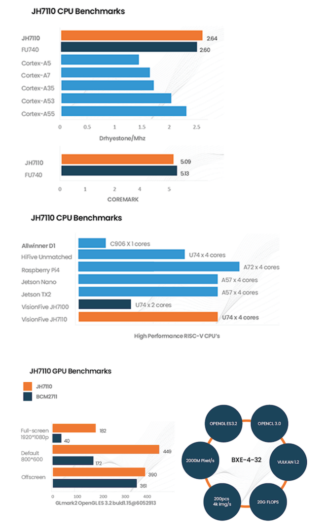
Some claims have the SiFive U74 core at 2.64 DMIPS/MHz (JH7110 SoC uses U74 cores).
https://allinfo.space/2022/08/28/visionfive-2-single-board-computer-with-risc-v-processor-and-3d-graphics-chip/
The Cortex-A53 and Cortex-A55 result is on the low side here but perfectly understandable as they need exceptional compiler support, especially for instruction scheduling. Take unscheduled code, like emu68 emulation 68k to RISC translated code, accessing memory linearly for example.
Cortex-A53 with 3 cycle load to use penalty
load pipe1
bubble pipe2
bubble pipe1 (3 cycle load-to-use penalty begin)
bubble pipe2
bubble pipe1
bubble pipe2
bubble pipe1
bubble pipe2 (3 cycle load-to-use penalty end)
op pipe1
load pipe2
bubble pipe1 (3 cycle load-to-use penalty begin)
bubble pipe2
bubble pipe1
bubble pipe2
bubble pipe1
bubble pipe2 (3 cycle load-to-use penalty end)
op pipe1
IPC=4/9=0.44
Cortex-A55 with 2 cycle load-to-use penalty
load pipe1
bubble pipe2
bubble pipe1 (2 cycle load-to-use penalty begin)
bubble pipe2
bubble pipe1
bubble pipe2 (2 cycle load-to-use penalty end)
op pipe1
load pipe2
bubble pipe1 (2 cycle load-to-use penalty begin)
bubble pipe2
bubble pipe1
bubble pipe2 (2 cycle load-to-use penalty end)
op pipe1
IPC=4/7=0.57
U74 with 0 cycle load-to-use penalty
load pipe1
bubble pipe2
op pipe1
load pipe2
op pipe1
IPC=4/3=1.33
68060 with 0 cycle load-to-use penalty
load+op pipe1
load+op pipe2
IPC=4/1=4 (actually 2 IPC but the equivalent of 4 RISC IPC)
The 68060 does not have a dual ported L1 data cache like x86 CPUs soon received but it does have a 4 way banked data cache which allows it often and is cheaper to implement in hardware. The SiFive U74 design is pure genius borrowed from long ago but the 68060 core with CISC ISA can still have roughly 3 times the performance when accessing memory. If the U74 core gained 0.5 DMIPS/MHz over the Cortex-A53 through improved memory performance, it is easy to see that the U74 core executing CISC instructions may reach 3 DMIPS/MHz. In any case, more real world performance is possible that doesn't require a compiler miracle.
This JH7110 SoC using U74 CPU cores in the VisionFive 2 SBC from StarFive, which was co-founded by SiFive, is very cool. They integrated an Imagination Technologies IMG BXE-4-32 MC4 GPU which is outperforming the BCM2711 RPi 4 GPU. This is far from Imagination Technologies best GPU but they do have an open source driver which is perhaps why it was tolerable for open standard hardware. Sadly, it does look like they removed big endian support in the GPU but it may be a customizable option and RISC-V is little endian.
https://doc-en.rvspace.org/VisionFive2/PDF/VisionFive2_Datasheet.pdf
The GPU does support OpenCL 3.0, OpenGL ES 3.2, and Vulkan 1.2 though. The CPU performance is less than RPi 4 but the U74 superscalar in-order CPU cores are more like the RPi 3 Cortex-A53. It is fanless and it looks like 15W is plenty for it. It has more purpose built embedded features including the one I suggested earlier.
https://doc-en.rvspace.org/JH7110/PDF/JH7110_Datasheet.pdf Quote:
Integrated 2 MB L2 Cache with ECC
o The L1 Instruction Cache and the L2 Cache can be configured into high-speed deterministic SRAMs
|
The SoC become a very nice microcontroller without external memory. Look at what the 68k AmigaOS could do with 2MiB of SRAM memory and better 68k code density. The AmigaOS is only a noncompetitive desktop OS for hardware systems that cost thousands of dollars while the VisionFive 2 was available for as cheap as $45 USD and is $89.99 USD for 8MiB version on Amazon.
https://www.amazon.com/VisionFive-RISC-V-StarFive-JH7110-Quad-core/dp/B0BGM6STN8
cdimauro Quote:
My point wasn't about o.s. code or user mode programs but only related to the features packed on the chip.
The 68851 (not 68451: I was recalling badly) is a very complex MMU which implementation costs a lot in terms of PPA. Especially if you take into account that you need two of them for a 2-way pipeline.
|
Other ISAs have different MMUs like PPC CPUs. There are somethings that are useless to keep because features were so rarely used. I suppose the 68020 CALLM/RTM instructions that I have never heard of anyone using should be implemented in hardware too?
cdimauro Quote:
Maybe I wasn't clear enough before. The point was/is that the Pentium brought the legacy from ALL predecessors (and also adding some modern features: see below) whereas it wasn't the same for the 68060.
So, you've to imagine the 68060 with everything carried on (and nothing removed. E.g.: not like it was for the 6840) from all predecessors. So, from the 68000 to 68040, adding the 68851 and 68882 with fully-fledged features & instructions.
Plus, if you want to put it on par with the Pentium in terms of new features, a 64 bit data bus, the machine registers to be added and especially the pipelined FPU.
I don't know how many transistors will be required for that (but I don't think that adding the transistors that you mentioned before could compensate it).
And I don't even know the impact of such changes on the performance (especially the reachable frequency) and power consumption. Here the 68851 implementation could play a big role.
|
Yea, Pentium kept all the baggage and garbage. That was a design choice in itself. The 68060 design simplified some while retaining good user mode compatibility. They removed too much in user mode but I don't have a problem with supervisor mode changes some of which is necessary. Full 68851 compatibility doesn't make sense and the exception frames are implementation and supervisor mode specific. I'll give you the pipelined FPU but it likely would have been lower in transistor cost than the Pentium increasing its integer pipeline depth. The 68060 still stays under 3 million transistors and has the option of increasing to a 16kiB I+D L1 with cheap 32 bit data bus which gives better performance than the Pentium with 8kiB I+D L1 and expensive 64 bit data bus.
cdimauro Quote:
No, but it's evident that the 68060 had itself some serious problems, even with the later revisions & more advanced processes.
It's more evident if you compare it to the Pentium using (roughly) the same process: the latter was able to reach much higher frequencies, despite the many more transistors bundled.
That's basically the same thing that happened to the 68040 (vs the 80486). And here there can be no "political reason" to justify it...
|
The 68040 problem was that it ran hot which limited how much it could be clocked up. The 80486 also ran hot but Intel persevered to raise the clock speed aided by economies of scale and higher margins in the desktop market. The 3.3V 68040V solved the heat issue but Motorola didn't even bother making a full version as Apple left the 68k desktop and laptop market. The 68060 was likely designated embedded only mid-development. Upper management probably considered cancelling the project but there was too much development time already so they likely ordered the team to get it out ASAP and as cheaply as possible. That is probably why it seems unfinished in areas. It probably also explains why it has trouble being clocked up. The pipeline stages need to balanced. Then the stages need to be analyzed and the bottlenecks of the slowest stages optimized. There was no effort to clock the cool 68060 up where there was a Herculean effort to clock up the hot 486 and Pentium. It wasn't just the total number of transistors that were a problem for x86 but also the active transistors, especially for the decoder. This is a much smaller percentage for x86-64 cores today because of the huge caches and large execution hardware but it was likely a problem for a scaled down x86 cores. It was also a problem for the Intel Atom as they tried to scale lower.
Last edited by matthey on 23-Nov-2023 at 11:18 PM.
|
| | Status: Offline |
| | Hammer
 | |
Re: The Case for the Complex Instruction Set Computer
Posted on 24-Nov-2023 4:28:18
| | [ #30 ] |
| |
|
Elite Member
|
Joined: 9-Mar-2003
Posts: 5339
From: Australia | | |
|
| @matthey
Quote:
The following are the actual 68060 stages of the instruction fetch pipeline.
68060
1. instruction address generation
2. instruction fetch
3. instruction early decode (to macro-ops with length decode)
4. instruction buffer (macro-op)
The following are possible x86(-64) stages based on side channel reverse engineering from the article above.
Intel x86(-64)
2. instruction fetch
3. instruction early decode (to macro-ops with length decode)
4. macro-op instruction buffer
5. decoder (macro-ops -> micro-ops)
6. instruction decode queue & micro-op cache
The decoupled execution pipelines would then execute the code placed in the buffer/queue at the end of these steps or stages. The 68060 is using fewer decoding stages and executing macro-ops instead of micro-ops like x86(-64). The 68060 only uses one (macro-op) instruction buffer while x86(-64) uses a macro-op buffer, micro-op buffer/queue and a micro-op cache which uses significant resources (the micro-op cache was the source of the vulnerability for this article too). Do you still think 68k instruction decoding is as difficult as x86(-64) decoding?
|
Modern X64 CPUs have a micro-op cache or trace cache e.g. AMD Zen-2 processors feature micro-op caches that can hold as many as 4K micro-ops and Zen 4 has 6.75K micro-ops.
The micro-op cache is inclusive with respect to the instruction cache and the instruction translation lookaside buffer (instruction TLB), which implies that any cache line evicted out of the instruction cache would also trigger an eviction in the micro-op cache.
For repeated instructions, micro-op caches lessen the workload on the front-end X86 decoders.
Quote:
There was no effort to clock the cool 68060 up where there was a Herculean effort to clock up the hot 486 and Pentium. It wasn't just the total number of transistors that were a problem for x86 but also the active transistors, especially for the decoder. This is a much smaller percentage for x86-64 cores today because of the huge caches and large execution hardware but it was likely a problem for a scaled down x86 cores. It was also a problem for the Intel Atom as they tried to scale lower.
|
Zen 4's micro-op cache can dispatch up to 9 macro-operations per clock cycle.
AMD's Threadripper 7980X's Zen 4C CPU core has 3.5 watts average and 0.85 volts. Threadripper 7980X uses a 5nm TSMC FinFET process.
Reference
https://youtu.be/yDEUOoWTzGw?t=512
Last edited by Hammer on 24-Nov-2023 at 04:47 AM.
Last edited by Hammer on 24-Nov-2023 at 04:37 AM.
Last edited by Hammer on 24-Nov-2023 at 04:30 AM.
Last edited by Hammer on 24-Nov-2023 at 04:29 AM.
_________________
Ryzen 9 7900X, DDR5-6000 64 GB RAM, GeForce RTX 4080 16 GB
Amiga 1200 (Rev 1D1, KS 3.2, PiStorm32lite/RPi 4B 4GB/Emu68)
Amiga 500 (Rev 6A, KS 3.2, PiStorm/RPi 3a/Emu68) |
| | Status: Offline |
| | Hammer
| |
Re: The Case for the Complex Instruction Set Computer
Posted on 24-Nov-2023 5:46:38
| | [ #31 ] |
| |
|
Elite Member
|
Joined: 9-Mar-2003
Posts: 5339
From: Australia | | |
|
| @matthey
Quote:
Both 68060 pipelines can superscalar execute very powerful instructions. As I recall, the Pentium has more restrictions on which instructions can execute together, isn't as good at shift or multiply and is more limited on superscalar issue with FPU instructions while the 68060 can superscalar execute an integer instruction in the sOEP with the FPU instruction (68060 mixed code performance makes up some ground on the fully pipelined Pentium FPU). The 68060 can not superscalar issue/execute instructions over 6 bytes in size which would improve performance. These larger instructions are not as common, especially in smaller and older programs, but it is better to keep even large immediates and displacements in a single instruction in the code. Large instructions are potentially more powerful and covering large address ranges is important as alternatives are worse.
|
Prove it with 68060 Rev 6 @ 100 Mhz with Quake benchmark.
The classic Pentium has a 64-bit bus to feed the CPU's dual 32-bit integer pipelines and the pipelined FPU.
Quake exploits Pentium's FDIV limited out-of-order feature i.e. while FDIV instruction is being processed, Pentium's FPU allows non-dependent instructions to continue execution.
https://www.youtube.com/watch?v=CuCHmney_Q4
Warp1260 playing Quake with 68060 100Mhz and CSGFX RTG.
https://youtu.be/0_dW-21gdkw?t=446
Warp1260's 50 vs 100 Mhz playing Quake benchmark
For demo2, 18.98 fps for 68060 @ 100 Mhz with RTG.
It's less the Pentium 100 and S3 Trio 64 results.
Last edited by Hammer on 24-Nov-2023 at 05:51 AM.
_________________
Ryzen 9 7900X, DDR5-6000 64 GB RAM, GeForce RTX 4080 16 GB
Amiga 1200 (Rev 1D1, KS 3.2, PiStorm32lite/RPi 4B 4GB/Emu68)
Amiga 500 (Rev 6A, KS 3.2, PiStorm/RPi 3a/Emu68) |
| | Status: Offline |
| | cdimauro
| |
Re: The Case for the Complex Instruction Set Computer
Posted on 24-Nov-2023 13:36:31
| | [ #32 ] |
| |
|
Elite Member
|
Joined: 29-Oct-2012
Posts: 3650
From: Germany | | |
|
| @matthey
Quote:
matthey wrote:
cdimauro Quote:
No: it's more advanced, with more resources, and supports more features.
|
If the SiFive U74 core is different for the reasons you give, is the ColdFire V5 core with 32kiB I+D cache, an extra pipeline stage added and hardware return stack added to what was derived from the 68060 design "more or less the same thing" as a 68060 and Pentium (P54C) core? Is the Pentium P55C which doubled the caches to 16kiB I+D, adds an extra pipeline stage and adds a hardware return stack, among other upgrades, still a Pentium core? |
They are all different to me, especially if we consider (and we should) the historical context, so when those processors were developed/released, the knowledge of the time, and the available fab processes.
Quote:
I've to say that that's really embarrassing for ARM.
SiFive's U74 core is a formidable performer despite its much simple in-order design.
That's something which could serves as a lesson for other processors vendors.
Quote:
The Cortex-A53 and Cortex-A55 result is on the low side here but perfectly understandable as they need exceptional compiler support, especially for instruction scheduling. Take unscheduled code, like emu68 emulation 68k to RISC translated code, accessing memory linearly for example.
Cortex-A53 with 3 cycle load to use penalty
load pipe1
bubble pipe2
bubble pipe1 (3 cycle load-to-use penalty begin)
bubble pipe2
bubble pipe1
bubble pipe2
bubble pipe1
bubble pipe2 (3 cycle load-to-use penalty end)
op pipe1
load pipe2
bubble pipe1 (3 cycle load-to-use penalty begin)
bubble pipe2
bubble pipe1
bubble pipe2
bubble pipe1
bubble pipe2 (3 cycle load-to-use penalty end)
op pipe1
IPC=4/9=0.44
Cortex-A55 with 2 cycle load-to-use penalty
load pipe1
bubble pipe2
bubble pipe1 (2 cycle load-to-use penalty begin)
bubble pipe2
bubble pipe1
bubble pipe2 (2 cycle load-to-use penalty end)
op pipe1
load pipe2
bubble pipe1 (2 cycle load-to-use penalty begin)
bubble pipe2
bubble pipe1
bubble pipe2 (2 cycle load-to-use penalty end)
op pipe1
IPC=4/7=0.57
U74 with 0 cycle load-to-use penalty
load pipe1
bubble pipe2
op pipe1
load pipe2
op pipe1
IPC=4/3=1.33
68060 with 0 cycle load-to-use penalty
load+op pipe1
load+op pipe2
IPC=4/1=4 (actually 2 IPC but the equivalent of 4 RISC IPC)
The 68060 does not have a dual ported L1 data cache like x86 CPUs soon received but it does have a 4 way banked data cache which allows it often and is cheaper to implement in hardware. The SiFive U74 design is pure genius borrowed from long ago but the 68060 core with CISC ISA can still have roughly 3 times the performance when accessing memory. If the U74 core gained 0.5 DMIPS/MHz over the Cortex-A53 through improved memory performance, it is easy to see that the U74 core executing CISC instructions may reach 3 DMIPS/MHz. In any case, more real world performance is possible that doesn't require a compiler miracle. |
Which shows why we agree that a CISC design has still something STRONG to say. Here is were we should bet.
Quote:
cdimauro Quote:
My point wasn't about o.s. code or user mode programs but only related to the features packed on the chip.
The 68851 (not 68451: I was recalling badly) is a very complex MMU which implementation costs a lot in terms of PPA. Especially if you take into account that you need two of them for a 2-way pipeline.
|
Other ISAs have different MMUs like PPC CPUs. There are somethings that are useless to keep because features were so rarely used. I suppose the 68020 CALLM/RTM instructions that I have never heard of anyone using should be implemented in hardware too? |
Exactly.
Quote:
cdimauro Quote:
Maybe I wasn't clear enough before. The point was/is that the Pentium brought the legacy from ALL predecessors (and also adding some modern features: see below) whereas it wasn't the same for the 68060.
So, you've to imagine the 68060 with everything carried on (and nothing removed. E.g.: not like it was for the 6840) from all predecessors. So, from the 68000 to 68040, adding the 68851 and 68882 with fully-fledged features & instructions.
Plus, if you want to put it on par with the Pentium in terms of new features, a 64 bit data bus, the machine registers to be added and especially the pipelined FPU.
I don't know how many transistors will be required for that (but I don't think that adding the transistors that you mentioned before could compensate it).
And I don't even know the impact of such changes on the performance (especially the reachable frequency) and power consumption. Here the 68851 implementation could play a big role.
|
Yea, Pentium kept all the baggage and garbage. That was a design choice in itself. |
Which paid: Intel was trustable because it guaranteed that even code developed 20 years back ran seemlessly on newer processors.
Backward-compatible was a great value which allowed developers and software houses to capitalize their investments.
Quote:
| The 68060 design simplified some while retaining good user mode compatibility. They removed too much in user mode but I don't have a problem with supervisor mode changes some of which is necessary. Full 68851 compatibility doesn't make sense and the exception frames are implementation and supervisor mode specific. |
Don't we have applications which run in supervisor mode? Yes, we had/have.
You can talk with ThoR and ask him what he thinks about all such changes which Motorola did on all its processors (there aren't two subsequent ones where the latter is 100% compatibile with the former).
Yes, supervisor code is much more rare compared to user mode one, but it's still there and needs to be written an maintained.
Maybe not that much on the Amiga land, but on more serious o.ses separating supervisor code from usermode code isn't about just executing a MOVE SR and setting and resetting the proper bit: it involves doing different things at the kernel and the driver level. And if you remove or change stuff in the supervisor mode, then you're in big troubles.
As I've said, backward-compatible is a value (well, it was much more in the past, at least), which Motorola decided to free itself and load to the developers shoulders.
Quote:
| I'll give you the pipelined FPU but it likely would have been lower in transistor cost than the Pentium increasing its integer pipeline depth. The 68060 still stays under 3 million transistors and has the option of increasing to a 16kiB I+D L1 with cheap 32 bit data bus which gives better performance than the Pentium with 8kiB I+D L1 and expensive 64 bit data bus. |
OK, maybe I wasn't still clear enough. The point was/isn't about : if remove this then I can do this, or if you give me this I can do this instead of this.
The point was that the 68060 had a better PPA compared to the Pentium because Motorola cut A LOT of things, by being not 100% backward-compatible. PLUS it missed some modern stuff (which Pentium introduced and 68060 didn't).
What do you think about this statement? Do you think that is if fair / plausible / realistic, or not?
Quote:
cdimauro Quote:
No, but it's evident that the 68060 had itself some serious problems, even with the later revisions & more advanced processes.
It's more evident if you compare it to the Pentium using (roughly) the same process: the latter was able to reach much higher frequencies, despite the many more transistors bundled.
That's basically the same thing that happened to the 68040 (vs the 80486). And here there can be no "political reason" to justify it...
|
The 68040 problem was that it ran hot which limited how much it could be clocked up. The 80486 also ran hot but Intel persevered to raise the clock speed aided by economies of scale and higher margins in the desktop market. The 3.3V 68040V solved the heat issue but Motorola didn't even bother making a full version as Apple left the 68k desktop and laptop market. The 68060 was likely designated embedded only mid-development. Upper management probably considered cancelling the project but there was too much development time already so they likely ordered the team to get it out ASAP and as cheaply as possible. That is probably why it seems unfinished in areas. It probably also explains why it has trouble being clocked up. The pipeline stages need to balanced. Then the stages need to be analyzed and the bottlenecks of the slowest stages optimized. There was no effort to clock the cool 68060 up where there was a Herculean effort to clock up the hot 486 and Pentium. |
OK, but... WHEN those projects (68040 and 68060) should have been completed and delivered then?
Because they were already late: the 80486 and the Pentium arrived one year BEFORE them and already started selling and creating a lot of pressure to Motorola.
You can't wait too much making a better product, because if you don't deliver then you don't get money and then you loose the market.
A clear example was Nintendo with its Nintendo64: it was really too late and Sony took the console market with its Playstation, which had a big advantage of 1.5 years.
Quote:
| It wasn't just the total number of transistors that were a problem for x86 but also the active transistors, especially for the decoder. |
But there were much less instructions and features at the time. Using some bitmaps to catch the prefixes doesn't require TONs of transistors, because of the 8 bit opcode(s).
68ks had a similar problem: catching the instructions which had the extension word so that it could be further checked to see if there are extra displacements. However using a bitmap having 16-bit opcodes isn't that convenient anymore (you need to do some tricks to reduce the size of the bitmap).
Both processor families had their own issues with instructions decoding, unfortunately.
On the topic, that's what Mitch Alsup said: https://groups.google.com/g/comp.arch/c/azcxvMRk2qA/m/FHya3V9cBwAJ
"There were two critical issues that concern the failure of the 68K family: one was technical, the other managerial.
The technical issue was that x86 was easier to pipeline than 68K and Intel got 486 out the door before Moto got a pipelined 68K out the door.
The managerial issue was that no manager in Moto was empowered to ever say yes to a good idea. This proved to be a greater burden than piplineability."
Quote:
| This is a much smaller percentage for x86-64 cores today because of the huge caches and large execution hardware but it was likely a problem for a scaled down x86 cores. It was also a problem for the Intel Atom as they tried to scale lower. |
Indeed. |
| | Status: Offline |
| | matthey
| |
Re: The Case for the Complex Instruction Set Computer
Posted on 26-Nov-2023 2:43:35
| | [ #33 ] |
| |
|
Elite Member
|
Joined: 14-Mar-2007
Posts: 2052
From: Kansas | | |
|
| cdimauro Quote:
I've to say that that's really embarrassing for ARM.
SiFive's U74 core is a formidable performer despite its much simple in-order design.
That's something which could serves as a lesson for other processors vendors.
|
AArch64 used more powerful CISC like addressing modes but I wasn't expecting RISC-V to counter by using a more powerful CISC like execution pipeline. Granted, they still have a ways to go to reach a CISC level of performance after the 4th ISA attempt from ARM and 5th ISA attempt from RISC-V. What else is there left to borrow besides reg-mem accesses without admitting defeat?
cdimauro Quote:
Which shows why we agree that a CISC design has still something STRONG to say. Here is were we should bet.
|
Is it better to bet on CISC or better to bet on CISC continuing to be ignored due to RISC propaganda?
cdimauro Quote:
Which paid: Intel was trustable because it guaranteed that even code developed 20 years back ran seemlessly on newer processors.
Backward-compatible was a great value which allowed developers and software houses to capitalize their investments.
|
Compatibility is important as I've preached before. Compatibility benefited x86 and lack of compatibility hurt the 68k and ColdFire although it didn't kill them. I believe some loss of compatibility is acceptable if it is reasonable, even in user mode. Not only is implementing CALLM/RTM wasteful but MOVE16 was obviously hardware specific which is why no compiler I know of uses these instructions. The 68060 especially cut compatibility too far even for the embedded market.
cdimauro Quote:
Don't we have applications which run in supervisor mode? Yes, we had/have.
You can talk with ThoR and ask him what he thinks about all such changes which Motorola did on all its processors (there aren't two subsequent ones where the latter is 100% compatibile with the former).
Yes, supervisor code is much more rare compared to user mode one, but it's still there and needs to be written an maintained.
Maybe not that much on the Amiga land, but on more serious o.ses separating supervisor code from usermode code isn't about just executing a MOVE SR and setting and resetting the proper bit: it involves doing different things at the kernel and the driver level. And if you remove or change stuff in the supervisor mode, then you're in big troubles.
As I've said, backward-compatible is a value (well, it was much more in the past, at least), which Motorola decided to free itself and load to the developers shoulders.
|
I have a pretty good idea what ThoR's opinion is. He understands logical changes but some changes are not logical considering the minor gain.
cdimauro Quote:
OK, maybe I wasn't still clear enough. The point was/isn't about : if remove this then I can do this, or if you give me this I can do this instead of this.
The point was that the 68060 had a better PPA compared to the Pentium because Motorola cut A LOT of things, by being not 100% backward-compatible. PLUS it missed some modern stuff (which Pentium introduced and 68060 didn't).
What do you think about this statement? Do you think that is if fair / plausible / realistic, or not?
|
I maintain that the 68060 had a significant enough PPA advantage over the Pentium to be obvious. The 68060 has some features that the Pentium does not. While the Pentium has more high performance features, I would put the 68060 at the same tech level and it is better at efficiently using the resources that are available. The 68060 had an 8 stage pipeline while the equivalent Pentium had a 5 stage pipeline.
https://cs.stanford.edu/people/eroberts/courses/soco/projects/risc/pipelining/index.html Quote:
The more pipe stages there are, the faster the pipeline is because each stage is then shorter. Ideally, a pipeline with five stages should be five times faster than a non-pipelined processor (or rather, a pipeline with one stage). The instructions are executed at the speed at which each stage is completed, and each stage takes one fifth of the amount of time that the non-pipelined instruction takes.
|
Increasing the pipeline stages adds active transistors and the Pentium already ran hot. More stages were added after die shrinks. A fully pipelined 68060 FPU could use power gating a much higher percentage of the time.
https://en.wikipedia.org/wiki/Power_gating
Even if a 68060 pipelined FPU and more compatibility features increased power by 10%-20% and transistors increased to 3 million, the P54C Pentium would still use at least 50% more power than the 68060. The P54C Pentium uses over 70% more power than the 68060 at the same frequency!
Pentium@75MHz P54C, 3.3V, 0.6um, 3.2 million transistors, 9.5W max
68060@75MHz 3.3V, 0.6um, 2.5 million transistors, ~5.5W max*
* estimate based on 68060@50MHz 3.9W max, 68060@66MHz 4.9W max
Performance is close but PPA is not close!
cdimauro Quote:
OK, but... WHEN those projects (68040 and 68060) should have been completed and delivered then?
Because they were already late: the 80486 and the Pentium arrived one year BEFORE them and already started selling and creating a lot of pressure to Motorola.
You can't wait too much making a better product, because if you don't deliver then you don't get money and then you loose the market.
A clear example was Nintendo with its Nintendo64: it was really too late and Sony took the console market with its Playstation, which had a big advantage of 1.5 years.
|
Motorola had management issues and a lack of management vision (6502 should have come out of Motorola too). They had good engineers/architects though. Sound like C=?
It was the 68040 which set the 68k product pipeline back. The following article about the 68060 mentions all the missed 68040 deadlines but also mentions an actual 68060@66MHz chip being tested in 1994 yet 68060@60MHz was the highest rated I've seen and they are rare.
https://websrv.cecs.uci.edu/~papers/mpr/MPR/ARTICLES/080502.pdf Quote:
Tests also showed that a 50-MHz 060 had 2.1 times the performance of a 40-MHz 040 running the Macintosh Speedometer benchmark; the 66-MHz version achieved a rating 2.8 times the 040. These figures are from alpha-test sites using actual 060 silicon installed in converted Macintosh machines and in Motorolas IDP (Integrated Development Platform) evaluation boards.
...
Process improvements will bring further speed gains and, perhaps more important, cost reduction.
|
The article claims 90 Dhrystone MIPS at 50 MHz which is 1.8 DMIPS/MHz while the P54C is listed at 1.38 DMIPS/MHz. "The 060 delivers better price/performance than Pentium but is beaten by PowerPC." even though the 68060 also uses fewer transistors than the PPC 601 and the deeper pipeline of the 68060 should have allowed it to be clocked up more improving the price/performance. It's very easy to make a chip noncompetitive by not allowing it to be clocked up. The article is correct though that the destiny of the 68060 was already decided which was the low clocked embedded market.
cdimauro Quote:
But there were much less instructions and features at the time. Using some bitmaps to catch the prefixes doesn't require TONs of transistors, because of the 8 bit opcode(s).
68ks had a similar problem: catching the instructions which had the extension word so that it could be further checked to see if there are extra displacements. However using a bitmap having 16-bit opcodes isn't that convenient anymore (you need to do some tricks to reduce the size of the bitmap).
Both processor families had their own issues with instructions decoding, unfortunately.
On the topic, that's what Mitch Alsup said: https://groups.google.com/g/comp.arch/c/azcxvMRk2qA/m/FHya3V9cBwAJ
"There were two critical issues that concern the failure of the 68K family: one was technical, the other managerial.
The technical issue was that x86 was easier to pipeline than 68K and Intel got 486 out the door before Moto got a pipelined 68K out the door.
The managerial issue was that no manager in Moto was empowered to ever say yes to a good idea. This proved to be a greater burden than piplineability."
|
The x86 ISA had shorter instructions and a smaller max instruction size than the 68k which allowed smaller and easier to pipeline cores. The inefficient x86 encoding map and only 8 GP registers caused too many instructions with too much memory traffic though. The x86-64 ISA gave fewer and larger instructions, more GP registers and reduced memory traffic but can't scale to as small of cores. The 68060 scales smaller than x86-64 where an in-order x86-64 core isn't even competitive anymore because of the size/area. The x86, x86-64 and 68k all have different advantages and different challenges to overcome but I would take the 68k any day. One of the 68k solutions was the decoupled instruction fetch pipeline and instruction execution pipelines with instruction buffer between. This meant that large instructions that required long decoding times usually did not affect execution performance. Most 68k and ColdFire CPU designs after the 68040 used this feature including 68060 and ColdFire V3 to V5. The 2 stage ColdFire V2 did not get this feature as the small instruction buffer adds a small cost that limits scaling to as small of cores. Mitch Alsup was an architect for an x86(-64) AMD CPU so he knows those solutions well. He defends the prefix decoding as not being as complex as RISC propaganda claims. Each prefix decoding is simple enough by itself. It is the out of control prefixes that are the x86-64 decoding problem. Decoupled pipelines with instruction buffers give a similar advantage for x86-64 core designs to usually hide long decoding times but it doesn't help with what I expect is greater decoding power used.
Last edited by matthey on 26-Nov-2023 at 06:37 AM.
|
| | Status: Offline |
| | cdimauro
| |
Re: The Case for the Complex Instruction Set Computer
Posted on 30-Nov-2023 18:06:38
| | [ #34 ] |
| |
|
Elite Member
|
Joined: 29-Oct-2012
Posts: 3650
From: Germany | | |
|
| @matthey
Quote:
matthey wrote:
cdimauro Quote:
I've to say that that's really embarrassing for ARM.
SiFive's U74 core is a formidable performer despite its much simple in-order design.
That's something which could serves as a lesson for other processors vendors.
|
AArch64 used more powerful CISC like addressing modes but I wasn't expecting RISC-V to counter by using a more powerful CISC like execution pipeline. Granted, they still have a ways to go to reach a CISC level of performance after the 4th ISA attempt from ARM and 5th ISA attempt from RISC-V. What else is there left to borrow besides reg-mem accesses without admitting defeat? |
They (academics) will never do it, like Fonzarelli.
Quote:
cdimauro Quote:
Which shows why we agree that a CISC design has still something STRONG to say. Here is were we should bet.
|
Is it better to bet on CISC or better to bet on CISC continuing to be ignored due to RISC propaganda? |
Rhetorical questions, to me.
Quote:
cdimauro Quote:
Which paid: Intel was trustable because it guaranteed that even code developed 20 years back ran seemlessly on newer processors.
Backward-compatible was a great value which allowed developers and software houses to capitalize their investments.
|
Compatibility is important as I've preached before. Compatibility benefited x86 and lack of compatibility hurt the 68k and ColdFire although it didn't kill them. I believe some loss of compatibility is acceptable if it is reasonable, even in user mode. Not only is implementing CALLM/RTM wasteful but MOVE16 was obviously hardware specific which is why no compiler I know of uses these instructions. The 68060 especially cut compatibility too far even for the embedded market. |
Just to be clear, I'm not a big fan of keeping compatibility 'til the death: when too much legacy / bad design decisions accumulated, then it's better to cut some burden or even restart (not necessarily 100% from scratch).
That's why I've designed my C64K not being 100% 68k-compatible, for example.
Quote:
cdimauro Quote:
OK, maybe I wasn't still clear enough. The point was/isn't about : if remove this then I can do this, or if you give me this I can do this instead of this.
The point was that the 68060 had a better PPA compared to the Pentium because Motorola cut A LOT of things, by being not 100% backward-compatible. PLUS it missed some modern stuff (which Pentium introduced and 68060 didn't).
What do you think about this statement? Do you think that is if fair / plausible / realistic, or not?
|
I maintain that the 68060 had a significant enough PPA advantage over the Pentium to be obvious. The 68060 has some features that the Pentium does not. While the Pentium has more high performance features, I would put the 68060 at the same tech level and it is better at efficiently using the resources that are available. The 68060 had an 8 stage pipeline while the equivalent Pentium had a 5 stage pipeline.
https://cs.stanford.edu/people/eroberts/courses/soco/projects/risc/pipelining/index.html Quote:
The more pipe stages there are, the faster the pipeline is because each stage is then shorter. Ideally, a pipeline with five stages should be five times faster than a non-pipelined processor (or rather, a pipeline with one stage). The instructions are executed at the speed at which each stage is completed, and each stage takes one fifth of the amount of time that the non-pipelined instruction takes.
|
Increasing the pipeline stages adds active transistors and the Pentium already ran hot. More stages were added after die shrinks. A fully pipelined 68060 FPU could use power gating a much higher percentage of the time.
https://en.wikipedia.org/wiki/Power_gating
Even if a 68060 pipelined FPU and more compatibility features increased power by 10%-20% and transistors increased to 3 million, the P54C Pentium would still use at least 50% more power than the 68060. The P54C Pentium uses over 70% more power than the 68060 at the same frequency!
Pentium@75MHz P54C, 3.3V, 0.6um, 3.2 million transistors, 9.5W max
68060@75MHz 3.3V, 0.6um, 2.5 million transistors, ~5.5W max*
* estimate based on 68060@50MHz 3.9W max, 68060@66MHz 4.9W max
Performance is close but PPA is not close! |
But that happens because... Motorola cut A LOT of stuff from the 68060 (and from is predecessors). That's the point for the whole (sub)discussion.
Quote:
cdimauro Quote:
OK, but... WHEN those projects (68040 and 68060) should have been completed and delivered then?
Because they were already late: the 80486 and the Pentium arrived one year BEFORE them and already started selling and creating a lot of pressure to Motorola.
You can't wait too much making a better product, because if you don't deliver then you don't get money and then you loose the market.
A clear example was Nintendo with its Nintendo64: it was really too late and Sony took the console market with its Playstation, which had a big advantage of 1.5 years.
|
Motorola had management issues and a lack of management vision (6502 should have come out of Motorola too). They had good engineers/architects though. Sound like C=?
It was the 68040 which set the 68k product pipeline back. The following article about the 68060 mentions all the missed 68040 deadlines but also mentions an actual 68060@66MHz chip being tested in 1994 yet 68060@60MHz was the highest rated I've seen and they are rare.
https://websrv.cecs.uci.edu/~papers/mpr/MPR/ARTICLES/080502.pdf Quote:
Tests also showed that a 50-MHz 060 had 2.1 times the performance of a 40-MHz 040 running the Macintosh Speedometer benchmark; the 66-MHz version achieved a rating 2.8 times the 040. These figures are from alpha-test sites using actual 060 silicon installed in converted Macintosh machines and in Motorolas IDP (Integrated Development Platform) evaluation boards.
...
Process improvements will bring further speed gains and, perhaps more important, cost reduction.
|
The article claims 90 Dhrystone MIPS at 50 MHz which is 1.8 DMIPS/MHz while the P54C is listed at 1.38 DMIPS/MHz. "The 060 delivers better price/performance than Pentium but is beaten by PowerPC." even though the 68060 also uses fewer transistors than the PPC 601 and the deeper pipeline of the 68060 should have allowed it to be clocked up more improving the price/performance. It's very easy to make a chip noncompetitive by not allowing it to be clocked up. The article is correct though that the destiny of the 68060 was already decided which was the low clocked embedded market. |
So, a political decision? I'm not sure about it.
As I've said, 68060s had issues trying to overclock them. This shows intrinsic issues of the chips design, which prevents to scale up with the clock.
A political decision is that you decide to sell a processor to max 50Mhz despite that you can reach 66Mhz. But people can find that it can run much higher by overclocking it...
Quote:
cdimauro Quote:
But there were much less instructions and features at the time. Using some bitmaps to catch the prefixes doesn't require TONs of transistors, because of the 8 bit opcode(s).
68ks had a similar problem: catching the instructions which had the extension word so that it could be further checked to see if there are extra displacements. However using a bitmap having 16-bit opcodes isn't that convenient anymore (you need to do some tricks to reduce the size of the bitmap).
Both processor families had their own issues with instructions decoding, unfortunately.
On the topic, that's what Mitch Alsup said: https://groups.google.com/g/comp.arch/c/azcxvMRk2qA/m/FHya3V9cBwAJ
"There were two critical issues that concern the failure of the 68K family: one was technical, the other managerial.
The technical issue was that x86 was easier to pipeline than 68K and Intel got 486 out the door before Moto got a pipelined 68K out the door.
The managerial issue was that no manager in Moto was empowered to ever say yes to a good idea. This proved to be a greater burden than piplineability."
|
The x86 ISA had shorter instructions and a smaller max instruction size than the 68k which allowed smaller and easier to pipeline cores. The inefficient x86 encoding map and only 8 GP registers caused too many instructions with too much memory traffic though. The x86-64 ISA gave fewer and larger instructions, more GP registers and reduced memory traffic but can't scale to as small of cores. The 68060 scales smaller than x86-64 where an in-order x86-64 core isn't even competitive anymore because of the size/area. The x86, x86-64 and 68k all have different advantages and different challenges to overcome but I would take the 68k any day. One of the 68k solutions was the decoupled instruction fetch pipeline and instruction execution pipelines with instruction buffer between. This meant that large instructions that required long decoding times usually did not affect execution performance. Most 68k and ColdFire CPU designs after the 68040 used this feature including 68060 and ColdFire V3 to V5. The 2 stage ColdFire V2 did not get this feature as the small instruction buffer adds a small cost that limits scaling to as small of cores. Mitch Alsup was an architect for an x86(-64) AMD CPU so he knows those solutions well. He defends the prefix decoding as not being as complex as RISC propaganda claims. Each prefix decoding is simple enough by itself. It is the out of control prefixes that are the x86-64 decoding problem. Decoupled pipelines with instruction buffers give a similar advantage for x86-64 core designs to usually hide long decoding times but it doesn't help with what I expect is greater decoding power used.
|
Having longer pipelines nowadays is pretty common, so it's not a big problem anymore to hide the more complex decoding of (legacy) CISCs.
However there are still many transistors that are active and which draw a lot of power. That's the main issue, I think.
Regarding the 68k vs x86/x64, it's difficult to make a comparison when there are so many different variables. I mean: ideally you should implement the same features on both processors and then you can evaluate how many transistors were used, how much power they consume, how high they can clock, and how much they perform.
But I don't think that something like that would ever be done, unfortunately. |
| | Status: Offline |
| |
|
|
|
[ home ][ about us ][ privacy ]
[ forums ][ classifieds ]
[ links ][ news archive ]
[ link to us ][ user account ]
|
